专家您好: 现在我调试代码发现AD采样有问题,我用的是28033.
我现在使用的一个基本情况是:
//AD初始化
void adcInit(void)
{
// The ADC resets to the ADC off state. When powering up the ADC, use the
// following sequence:
// 1) If external reference is desired, enable this mode using bits 15-14 in the
// ADCREFSEL Register. This mode must be enabled before band gap is
// powered.
// 2) Power up the reference, bandgap, and analog circuits together by setting
// bits 7-5 (ADCBGRFDN1, ADCBGRFDN0, ADCPWDN) in the ADCTRL3
// register.
// 3) Before performing the first conversion, a delay of 5 ms is required.
// When powering down the ADC, all three bits can be cleared simultaneously.
// The ADC power level must be controlled via software and they are
// independent of the state of the device power modes.
EALLOW;
SysCtrlRegs.PCLKCR0.bit.ADCENCLK = 1;
(*Device_cal)();
EDIS;
EALLOW;
AdcRegs.ADCCTL1.bit.ADCPWDN = 1; // Power ADC
AdcRegs.ADCCTL1.bit.ADCBGPWD = 1; // Power ADC BG
AdcRegs.ADCCTL1.bit.ADCREFPWD = 1; // Power reference
AdcRegs.ADCCTL1.bit.ADCENABLE = 1; // Enable ADC
AdcRegs.ADCCTL1.bit.ADCREFSEL = 0; // 0–internal reference
EDIS;
DELAY_US(ADC_usDELAY);// Delay after powering up ADC 1000L
EALLOW;
//control set
AdcRegs.ADCCTL1.bit.INTPULSEPOS = 1; //ADCINT1s trigger at end of conversion
AdcRegs.INTSEL1N2.bit.INT1SEL = 5; //EOC5 triggers ADCINT1
AdcRegs.INTSEL1N2.bit.INT1E = 1; //Enable ADCINT1
AdcRegs.ADCSAMPLEMODE.all=0x00FF; //Simultaneous sample
//SOC0/SOC1–A1:RESULT0 B1:RESULT1–
AdcRegs.ADCSOC0CTL.bit.ACQPS = 6;//sample window
AdcRegs.ADCSOC0CTL.bit.CHSEL = 1; //SOC0/SOC1–channel select 1
AdcRegs.ADCSOC0CTL.bit.TRIGSEL = 5;//triggle source PWM1SOCA
//SOC2/SOC3–A1:RESULT2 B1:RESULT3—
AdcRegs.ADCSOC2CTL.bit.ACQPS = 6;//sample window
AdcRegs.ADCSOC2CTL.bit.CHSEL = 2; //SOC2/SOC3–channel select 1
AdcRegs.ADCSOC2CTL.bit.TRIGSEL = 5;//triggle source PWM1SOCA
//SOC4/SOC5–A0:RESULT4 B0:RESULT5–
AcRegs.ADCSOC4CTL.bit.ACQPS = 6;//sample window
AdcRegs.ADCSOC4CTL.bit.CHSEL = 0; //SOC4/SOC5–channel select 0
AdcRegs.ADCSOC4CTL.bit.TRIGSEL = 5;//triggle source PWM1SOCA
EDIS;
}
然后在中断中去读取AD结果寄存器的值,
发现在最初的前几十个中断中读到的AD值是错误的,硬件的AD口用示波器看是没有异常的。
想请教下专家,这时候除了看AD这块的配置,还需要关注其他哪里?
谢谢
Eric Ma:
请问你查看的AD值是所有的通道都有问题吗?
目前初步建议:
1. ACQPS 全部改成9.
2. SOC0和SOC1的结果不要读。
以上两点见芯片勘误表。
3. 参考芯片在controlSUITE的例程去测试。
ERIC
专家您好: 现在我调试代码发现AD采样有问题,我用的是28033.
我现在使用的一个基本情况是:
//AD初始化
void adcInit(void)
{
// The ADC resets to the ADC off state. When powering up the ADC, use the
// following sequence:
// 1) If external reference is desired, enable this mode using bits 15-14 in the
// ADCREFSEL Register. This mode must be enabled before band gap is
// powered.
// 2) Power up the reference, bandgap, and analog circuits together by setting
// bits 7-5 (ADCBGRFDN1, ADCBGRFDN0, ADCPWDN) in the ADCTRL3
// register.
// 3) Before performing the first conversion, a delay of 5 ms is required.
// When powering down the ADC, all three bits can be cleared simultaneously.
// The ADC power level must be controlled via software and they are
// independent of the state of the device power modes.
EALLOW;
SysCtrlRegs.PCLKCR0.bit.ADCENCLK = 1;
(*Device_cal)();
EDIS;
EALLOW;
AdcRegs.ADCCTL1.bit.ADCPWDN = 1; // Power ADC
AdcRegs.ADCCTL1.bit.ADCBGPWD = 1; // Power ADC BG
AdcRegs.ADCCTL1.bit.ADCREFPWD = 1; // Power reference
AdcRegs.ADCCTL1.bit.ADCENABLE = 1; // Enable ADC
AdcRegs.ADCCTL1.bit.ADCREFSEL = 0; // 0–internal reference
EDIS;
DELAY_US(ADC_usDELAY);// Delay after powering up ADC 1000L
EALLOW;
//control set
AdcRegs.ADCCTL1.bit.INTPULSEPOS = 1; //ADCINT1s trigger at end of conversion
AdcRegs.INTSEL1N2.bit.INT1SEL = 5; //EOC5 triggers ADCINT1
AdcRegs.INTSEL1N2.bit.INT1E = 1; //Enable ADCINT1
AdcRegs.ADCSAMPLEMODE.all=0x00FF; //Simultaneous sample
//SOC0/SOC1–A1:RESULT0 B1:RESULT1–
AdcRegs.ADCSOC0CTL.bit.ACQPS = 6;//sample window
AdcRegs.ADCSOC0CTL.bit.CHSEL = 1; //SOC0/SOC1–channel select 1
AdcRegs.ADCSOC0CTL.bit.TRIGSEL = 5;//triggle source PWM1SOCA
//SOC2/SOC3–A1:RESULT2 B1:RESULT3—
AdcRegs.ADCSOC2CTL.bit.ACQPS = 6;//sample window
AdcRegs.ADCSOC2CTL.bit.CHSEL = 2; //SOC2/SOC3–channel select 1
AdcRegs.ADCSOC2CTL.bit.TRIGSEL = 5;//triggle source PWM1SOCA
//SOC4/SOC5–A0:RESULT4 B0:RESULT5–
AcRegs.ADCSOC4CTL.bit.ACQPS = 6;//sample window
AdcRegs.ADCSOC4CTL.bit.CHSEL = 0; //SOC4/SOC5–channel select 0
AdcRegs.ADCSOC4CTL.bit.TRIGSEL = 5;//triggle source PWM1SOCA
EDIS;
}
然后在中断中去读取AD结果寄存器的值,
发现在最初的前几十个中断中读到的AD值是错误的,硬件的AD口用示波器看是没有异常的。
想请教下专家,这时候除了看AD这块的配置,还需要关注其他哪里?
谢谢
Young Hu:
您好!从代码上来看,除了采样窗需要调整下试试看,其他的没有什么问题。
另外,需要确认下硬件是不是真的有干扰,用示波器看的话,通道有电容滤波,真实情况可能也看不到。建议加一个稳定电压,如电池,直接接到引脚上去测试,确认代码没有问题。
专家您好: 现在我调试代码发现AD采样有问题,我用的是28033.
我现在使用的一个基本情况是:
//AD初始化
void adcInit(void)
{
// The ADC resets to the ADC off state. When powering up the ADC, use the
// following sequence:
// 1) If external reference is desired, enable this mode using bits 15-14 in the
// ADCREFSEL Register. This mode must be enabled before band gap is
// powered.
// 2) Power up the reference, bandgap, and analog circuits together by setting
// bits 7-5 (ADCBGRFDN1, ADCBGRFDN0, ADCPWDN) in the ADCTRL3
// register.
// 3) Before performing the first conversion, a delay of 5 ms is required.
// When powering down the ADC, all three bits can be cleared simultaneously.
// The ADC power level must be controlled via software and they are
// independent of the state of the device power modes.
EALLOW;
SysCtrlRegs.PCLKCR0.bit.ADCENCLK = 1;
(*Device_cal)();
EDIS;
EALLOW;
AdcRegs.ADCCTL1.bit.ADCPWDN = 1; // Power ADC
AdcRegs.ADCCTL1.bit.ADCBGPWD = 1; // Power ADC BG
AdcRegs.ADCCTL1.bit.ADCREFPWD = 1; // Power reference
AdcRegs.ADCCTL1.bit.ADCENABLE = 1; // Enable ADC
AdcRegs.ADCCTL1.bit.ADCREFSEL = 0; // 0–internal reference
EDIS;
DELAY_US(ADC_usDELAY);// Delay after powering up ADC 1000L
EALLOW;
//control set
AdcRegs.ADCCTL1.bit.INTPULSEPOS = 1; //ADCINT1s trigger at end of conversion
AdcRegs.INTSEL1N2.bit.INT1SEL = 5; //EOC5 triggers ADCINT1
AdcRegs.INTSEL1N2.bit.INT1E = 1; //Enable ADCINT1
AdcRegs.ADCSAMPLEMODE.all=0x00FF; //Simultaneous sample
//SOC0/SOC1–A1:RESULT0 B1:RESULT1–
AdcRegs.ADCSOC0CTL.bit.ACQPS = 6;//sample window
AdcRegs.ADCSOC0CTL.bit.CHSEL = 1; //SOC0/SOC1–channel select 1
AdcRegs.ADCSOC0CTL.bit.TRIGSEL = 5;//triggle source PWM1SOCA
//SOC2/SOC3–A1:RESULT2 B1:RESULT3—
AdcRegs.ADCSOC2CTL.bit.ACQPS = 6;//sample window
AdcRegs.ADCSOC2CTL.bit.CHSEL = 2; //SOC2/SOC3–channel select 1
AdcRegs.ADCSOC2CTL.bit.TRIGSEL = 5;//triggle source PWM1SOCA
//SOC4/SOC5–A0:RESULT4 B0:RESULT5–
AcRegs.ADCSOC4CTL.bit.ACQPS = 6;//sample window
AdcRegs.ADCSOC4CTL.bit.CHSEL = 0; //SOC4/SOC5–channel select 0
AdcRegs.ADCSOC4CTL.bit.TRIGSEL = 5;//triggle source PWM1SOCA
EDIS;
}
然后在中断中去读取AD结果寄存器的值,
发现在最初的前几十个中断中读到的AD值是错误的,硬件的AD口用示波器看是没有异常的。
想请教下专家,这时候除了看AD这块的配置,还需要关注其他哪里?
谢谢
seven xie:
回复 Eric Ma:
您好:
1、2都试过,采样还是会有问题
至于3,之前外设驱动那块,是直接拿例程上的代码做的。
出现采样问题的时候,都是进入中断后,在一个固定时间发生。
还请专家帮忙想下,其他地方会不会影响采样?
专家您好: 现在我调试代码发现AD采样有问题,我用的是28033.
我现在使用的一个基本情况是:
//AD初始化
void adcInit(void)
{
// The ADC resets to the ADC off state. When powering up the ADC, use the
// following sequence:
// 1) If external reference is desired, enable this mode using bits 15-14 in the
// ADCREFSEL Register. This mode must be enabled before band gap is
// powered.
// 2) Power up the reference, bandgap, and analog circuits together by setting
// bits 7-5 (ADCBGRFDN1, ADCBGRFDN0, ADCPWDN) in the ADCTRL3
// register.
// 3) Before performing the first conversion, a delay of 5 ms is required.
// When powering down the ADC, all three bits can be cleared simultaneously.
// The ADC power level must be controlled via software and they are
// independent of the state of the device power modes.
EALLOW;
SysCtrlRegs.PCLKCR0.bit.ADCENCLK = 1;
(*Device_cal)();
EDIS;
EALLOW;
AdcRegs.ADCCTL1.bit.ADCPWDN = 1; // Power ADC
AdcRegs.ADCCTL1.bit.ADCBGPWD = 1; // Power ADC BG
AdcRegs.ADCCTL1.bit.ADCREFPWD = 1; // Power reference
AdcRegs.ADCCTL1.bit.ADCENABLE = 1; // Enable ADC
AdcRegs.ADCCTL1.bit.ADCREFSEL = 0; // 0–internal reference
EDIS;
DELAY_US(ADC_usDELAY);// Delay after powering up ADC 1000L
EALLOW;
//control set
AdcRegs.ADCCTL1.bit.INTPULSEPOS = 1; //ADCINT1s trigger at end of conversion
AdcRegs.INTSEL1N2.bit.INT1SEL = 5; //EOC5 triggers ADCINT1
AdcRegs.INTSEL1N2.bit.INT1E = 1; //Enable ADCINT1
AdcRegs.ADCSAMPLEMODE.all=0x00FF; //Simultaneous sample
//SOC0/SOC1–A1:RESULT0 B1:RESULT1–
AdcRegs.ADCSOC0CTL.bit.ACQPS = 6;//sample window
AdcRegs.ADCSOC0CTL.bit.CHSEL = 1; //SOC0/SOC1–channel select 1
AdcRegs.ADCSOC0CTL.bit.TRIGSEL = 5;//triggle source PWM1SOCA
//SOC2/SOC3–A1:RESULT2 B1:RESULT3—
AdcRegs.ADCSOC2CTL.bit.ACQPS = 6;//sample window
AdcRegs.ADCSOC2CTL.bit.CHSEL = 2; //SOC2/SOC3–channel select 1
AdcRegs.ADCSOC2CTL.bit.TRIGSEL = 5;//triggle source PWM1SOCA
//SOC4/SOC5–A0:RESULT4 B0:RESULT5–
AcRegs.ADCSOC4CTL.bit.ACQPS = 6;//sample window
AdcRegs.ADCSOC4CTL.bit.CHSEL = 0; //SOC4/SOC5–channel select 0
AdcRegs.ADCSOC4CTL.bit.TRIGSEL = 5;//triggle source PWM1SOCA
EDIS;
}
然后在中断中去读取AD结果寄存器的值,
发现在最初的前几十个中断中读到的AD值是错误的,硬件的AD口用示波器看是没有异常的。
想请教下专家,这时候除了看AD这块的配置,还需要关注其他哪里?
谢谢
seven xie:
回复 Young Hu:
正在仿真调试,因为采样有问题的时候,是最初中断开始后的一段时间,而且是固定时间发生的。
专家您好: 现在我调试代码发现AD采样有问题,我用的是28033.
我现在使用的一个基本情况是:
//AD初始化
void adcInit(void)
{
// The ADC resets to the ADC off state. When powering up the ADC, use the
// following sequence:
// 1) If external reference is desired, enable this mode using bits 15-14 in the
// ADCREFSEL Register. This mode must be enabled before band gap is
// powered.
// 2) Power up the reference, bandgap, and analog circuits together by setting
// bits 7-5 (ADCBGRFDN1, ADCBGRFDN0, ADCPWDN) in the ADCTRL3
// register.
// 3) Before performing the first conversion, a delay of 5 ms is required.
// When powering down the ADC, all three bits can be cleared simultaneously.
// The ADC power level must be controlled via software and they are
// independent of the state of the device power modes.
EALLOW;
SysCtrlRegs.PCLKCR0.bit.ADCENCLK = 1;
(*Device_cal)();
EDIS;
EALLOW;
AdcRegs.ADCCTL1.bit.ADCPWDN = 1; // Power ADC
AdcRegs.ADCCTL1.bit.ADCBGPWD = 1; // Power ADC BG
AdcRegs.ADCCTL1.bit.ADCREFPWD = 1; // Power reference
AdcRegs.ADCCTL1.bit.ADCENABLE = 1; // Enable ADC
AdcRegs.ADCCTL1.bit.ADCREFSEL = 0; // 0–internal reference
EDIS;
DELAY_US(ADC_usDELAY);// Delay after powering up ADC 1000L
EALLOW;
//control set
AdcRegs.ADCCTL1.bit.INTPULSEPOS = 1; //ADCINT1s trigger at end of conversion
AdcRegs.INTSEL1N2.bit.INT1SEL = 5; //EOC5 triggers ADCINT1
AdcRegs.INTSEL1N2.bit.INT1E = 1; //Enable ADCINT1
AdcRegs.ADCSAMPLEMODE.all=0x00FF; //Simultaneous sample
//SOC0/SOC1–A1:RESULT0 B1:RESULT1–
AdcRegs.ADCSOC0CTL.bit.ACQPS = 6;//sample window
AdcRegs.ADCSOC0CTL.bit.CHSEL = 1; //SOC0/SOC1–channel select 1
AdcRegs.ADCSOC0CTL.bit.TRIGSEL = 5;//triggle source PWM1SOCA
//SOC2/SOC3–A1:RESULT2 B1:RESULT3—
AdcRegs.ADCSOC2CTL.bit.ACQPS = 6;//sample window
AdcRegs.ADCSOC2CTL.bit.CHSEL = 2; //SOC2/SOC3–channel select 1
AdcRegs.ADCSOC2CTL.bit.TRIGSEL = 5;//triggle source PWM1SOCA
//SOC4/SOC5–A0:RESULT4 B0:RESULT5–
AcRegs.ADCSOC4CTL.bit.ACQPS = 6;//sample window
AdcRegs.ADCSOC4CTL.bit.CHSEL = 0; //SOC4/SOC5–channel select 0
AdcRegs.ADCSOC4CTL.bit.TRIGSEL = 5;//triggle source PWM1SOCA
EDIS;
}
然后在中断中去读取AD结果寄存器的值,
发现在最初的前几十个中断中读到的AD值是错误的,硬件的AD口用示波器看是没有异常的。
想请教下专家,这时候除了看AD这块的配置,还需要关注其他哪里?
谢谢
seven xie:
回复 Young Hu:
您好:
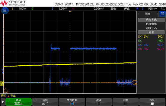
我直接把有问题的AD口接地,但是用IO口测试,还是会出问题:
当AD>限值时,IO口置高。见附件,持续35ms的高电平就是发送采样有问题的时刻,第一个7ms只是IO初始化时刻。
所以应该是软件有问题了。
专家您好: 现在我调试代码发现AD采样有问题,我用的是28033.
我现在使用的一个基本情况是:
//AD初始化
void adcInit(void)
{
// The ADC resets to the ADC off state. When powering up the ADC, use the
// following sequence:
// 1) If external reference is desired, enable this mode using bits 15-14 in the
// ADCREFSEL Register. This mode must be enabled before band gap is
// powered.
// 2) Power up the reference, bandgap, and analog circuits together by setting
// bits 7-5 (ADCBGRFDN1, ADCBGRFDN0, ADCPWDN) in the ADCTRL3
// register.
// 3) Before performing the first conversion, a delay of 5 ms is required.
// When powering down the ADC, all three bits can be cleared simultaneously.
// The ADC power level must be controlled via software and they are
// independent of the state of the device power modes.
EALLOW;
SysCtrlRegs.PCLKCR0.bit.ADCENCLK = 1;
(*Device_cal)();
EDIS;
EALLOW;
AdcRegs.ADCCTL1.bit.ADCPWDN = 1; // Power ADC
AdcRegs.ADCCTL1.bit.ADCBGPWD = 1; // Power ADC BG
AdcRegs.ADCCTL1.bit.ADCREFPWD = 1; // Power reference
AdcRegs.ADCCTL1.bit.ADCENABLE = 1; // Enable ADC
AdcRegs.ADCCTL1.bit.ADCREFSEL = 0; // 0–internal reference
EDIS;
DELAY_US(ADC_usDELAY);// Delay after powering up ADC 1000L
EALLOW;
//control set
AdcRegs.ADCCTL1.bit.INTPULSEPOS = 1; //ADCINT1s trigger at end of conversion
AdcRegs.INTSEL1N2.bit.INT1SEL = 5; //EOC5 triggers ADCINT1
AdcRegs.INTSEL1N2.bit.INT1E = 1; //Enable ADCINT1
AdcRegs.ADCSAMPLEMODE.all=0x00FF; //Simultaneous sample
//SOC0/SOC1–A1:RESULT0 B1:RESULT1–
AdcRegs.ADCSOC0CTL.bit.ACQPS = 6;//sample window
AdcRegs.ADCSOC0CTL.bit.CHSEL = 1; //SOC0/SOC1–channel select 1
AdcRegs.ADCSOC0CTL.bit.TRIGSEL = 5;//triggle source PWM1SOCA
//SOC2/SOC3–A1:RESULT2 B1:RESULT3—
AdcRegs.ADCSOC2CTL.bit.ACQPS = 6;//sample window
AdcRegs.ADCSOC2CTL.bit.CHSEL = 2; //SOC2/SOC3–channel select 1
AdcRegs.ADCSOC2CTL.bit.TRIGSEL = 5;//triggle source PWM1SOCA
//SOC4/SOC5–A0:RESULT4 B0:RESULT5–
AcRegs.ADCSOC4CTL.bit.ACQPS = 6;//sample window
AdcRegs.ADCSOC4CTL.bit.CHSEL = 0; //SOC4/SOC5–channel select 0
AdcRegs.ADCSOC4CTL.bit.TRIGSEL = 5;//triggle source PWM1SOCA
EDIS;
}
然后在中断中去读取AD结果寄存器的值,
发现在最初的前几十个中断中读到的AD值是错误的,硬件的AD口用示波器看是没有异常的。
想请教下专家,这时候除了看AD这块的配置,还需要关注其他哪里?
谢谢
Victor Zheng:
回复 seven xie:
您好 你的ADC采样遇到是什么问题?
采到的结果和,实际值差多少?
ADC引脚输入的信号是从哪里来的。建议直接送一个干电池的电压。这样可以排除信号的问题
你的电路板的AVCC是怎么供的,建议使用线性源输入来排除电源上的干扰。
如果你怀疑你的软件配置有问题,请用controlSUITE中的例程来测试。
专家您好: 现在我调试代码发现AD采样有问题,我用的是28033.
我现在使用的一个基本情况是:
//AD初始化
void adcInit(void)
{
// The ADC resets to the ADC off state. When powering up the ADC, use the
// following sequence:
// 1) If external reference is desired, enable this mode using bits 15-14 in the
// ADCREFSEL Register. This mode must be enabled before band gap is
// powered.
// 2) Power up the reference, bandgap, and analog circuits together by setting
// bits 7-5 (ADCBGRFDN1, ADCBGRFDN0, ADCPWDN) in the ADCTRL3
// register.
// 3) Before performing the first conversion, a delay of 5 ms is required.
// When powering down the ADC, all three bits can be cleared simultaneously.
// The ADC power level must be controlled via software and they are
// independent of the state of the device power modes.
EALLOW;
SysCtrlRegs.PCLKCR0.bit.ADCENCLK = 1;
(*Device_cal)();
EDIS;
EALLOW;
AdcRegs.ADCCTL1.bit.ADCPWDN = 1; // Power ADC
AdcRegs.ADCCTL1.bit.ADCBGPWD = 1; // Power ADC BG
AdcRegs.ADCCTL1.bit.ADCREFPWD = 1; // Power reference
AdcRegs.ADCCTL1.bit.ADCENABLE = 1; // Enable ADC
AdcRegs.ADCCTL1.bit.ADCREFSEL = 0; // 0–internal reference
EDIS;
DELAY_US(ADC_usDELAY);// Delay after powering up ADC 1000L
EALLOW;
//control set
AdcRegs.ADCCTL1.bit.INTPULSEPOS = 1; //ADCINT1s trigger at end of conversion
AdcRegs.INTSEL1N2.bit.INT1SEL = 5; //EOC5 triggers ADCINT1
AdcRegs.INTSEL1N2.bit.INT1E = 1; //Enable ADCINT1
AdcRegs.ADCSAMPLEMODE.all=0x00FF; //Simultaneous sample
//SOC0/SOC1–A1:RESULT0 B1:RESULT1–
AdcRegs.ADCSOC0CTL.bit.ACQPS = 6;//sample window
AdcRegs.ADCSOC0CTL.bit.CHSEL = 1; //SOC0/SOC1–channel select 1
AdcRegs.ADCSOC0CTL.bit.TRIGSEL = 5;//triggle source PWM1SOCA
//SOC2/SOC3–A1:RESULT2 B1:RESULT3—
AdcRegs.ADCSOC2CTL.bit.ACQPS = 6;//sample window
AdcRegs.ADCSOC2CTL.bit.CHSEL = 2; //SOC2/SOC3–channel select 1
AdcRegs.ADCSOC2CTL.bit.TRIGSEL = 5;//triggle source PWM1SOCA
//SOC4/SOC5–A0:RESULT4 B0:RESULT5–
AcRegs.ADCSOC4CTL.bit.ACQPS = 6;//sample window
AdcRegs.ADCSOC4CTL.bit.CHSEL = 0; //SOC4/SOC5–channel select 0
AdcRegs.ADCSOC4CTL.bit.TRIGSEL = 5;//triggle source PWM1SOCA
EDIS;
}
然后在中断中去读取AD结果寄存器的值,
发现在最初的前几十个中断中读到的AD值是错误的,硬件的AD口用示波器看是没有异常的。
想请教下专家,这时候除了看AD这块的配置,还需要关注其他哪里?
谢谢
seven xie:
回复 Young Hu:
您好:
AD结果寄存器能否初始化?
专家您好: 现在我调试代码发现AD采样有问题,我用的是28033.
我现在使用的一个基本情况是:
//AD初始化
void adcInit(void)
{
// The ADC resets to the ADC off state. When powering up the ADC, use the
// following sequence:
// 1) If external reference is desired, enable this mode using bits 15-14 in the
// ADCREFSEL Register. This mode must be enabled before band gap is
// powered.
// 2) Power up the reference, bandgap, and analog circuits together by setting
// bits 7-5 (ADCBGRFDN1, ADCBGRFDN0, ADCPWDN) in the ADCTRL3
// register.
// 3) Before performing the first conversion, a delay of 5 ms is required.
// When powering down the ADC, all three bits can be cleared simultaneously.
// The ADC power level must be controlled via software and they are
// independent of the state of the device power modes.
EALLOW;
SysCtrlRegs.PCLKCR0.bit.ADCENCLK = 1;
(*Device_cal)();
EDIS;
EALLOW;
AdcRegs.ADCCTL1.bit.ADCPWDN = 1; // Power ADC
AdcRegs.ADCCTL1.bit.ADCBGPWD = 1; // Power ADC BG
AdcRegs.ADCCTL1.bit.ADCREFPWD = 1; // Power reference
AdcRegs.ADCCTL1.bit.ADCENABLE = 1; // Enable ADC
AdcRegs.ADCCTL1.bit.ADCREFSEL = 0; // 0–internal reference
EDIS;
DELAY_US(ADC_usDELAY);// Delay after powering up ADC 1000L
EALLOW;
//control set
AdcRegs.ADCCTL1.bit.INTPULSEPOS = 1; //ADCINT1s trigger at end of conversion
AdcRegs.INTSEL1N2.bit.INT1SEL = 5; //EOC5 triggers ADCINT1
AdcRegs.INTSEL1N2.bit.INT1E = 1; //Enable ADCINT1
AdcRegs.ADCSAMPLEMODE.all=0x00FF; //Simultaneous sample
//SOC0/SOC1–A1:RESULT0 B1:RESULT1–
AdcRegs.ADCSOC0CTL.bit.ACQPS = 6;//sample window
AdcRegs.ADCSOC0CTL.bit.CHSEL = 1; //SOC0/SOC1–channel select 1
AdcRegs.ADCSOC0CTL.bit.TRIGSEL = 5;//triggle source PWM1SOCA
//SOC2/SOC3–A1:RESULT2 B1:RESULT3—
AdcRegs.ADCSOC2CTL.bit.ACQPS = 6;//sample window
AdcRegs.ADCSOC2CTL.bit.CHSEL = 2; //SOC2/SOC3–channel select 1
AdcRegs.ADCSOC2CTL.bit.TRIGSEL = 5;//triggle source PWM1SOCA
//SOC4/SOC5–A0:RESULT4 B0:RESULT5–
AcRegs.ADCSOC4CTL.bit.ACQPS = 6;//sample window
AdcRegs.ADCSOC4CTL.bit.CHSEL = 0; //SOC4/SOC5–channel select 0
AdcRegs.ADCSOC4CTL.bit.TRIGSEL = 5;//triggle source PWM1SOCA
EDIS;
}
然后在中断中去读取AD结果寄存器的值,
发现在最初的前几十个中断中读到的AD值是错误的,硬件的AD口用示波器看是没有异常的。
想请教下专家,这时候除了看AD这块的配置,还需要关注其他哪里?
谢谢
Victor Zheng:
回复 seven xie:
您好
ADC结果寄存器是只读的。无法写入。
专家您好: 现在我调试代码发现AD采样有问题,我用的是28033.
我现在使用的一个基本情况是:
//AD初始化
void adcInit(void)
{
// The ADC resets to the ADC off state. When powering up the ADC, use the
// following sequence:
// 1) If external reference is desired, enable this mode using bits 15-14 in the
// ADCREFSEL Register. This mode must be enabled before band gap is
// powered.
// 2) Power up the reference, bandgap, and analog circuits together by setting
// bits 7-5 (ADCBGRFDN1, ADCBGRFDN0, ADCPWDN) in the ADCTRL3
// register.
// 3) Before performing the first conversion, a delay of 5 ms is required.
// When powering down the ADC, all three bits can be cleared simultaneously.
// The ADC power level must be controlled via software and they are
// independent of the state of the device power modes.
EALLOW;
SysCtrlRegs.PCLKCR0.bit.ADCENCLK = 1;
(*Device_cal)();
EDIS;
EALLOW;
AdcRegs.ADCCTL1.bit.ADCPWDN = 1; // Power ADC
AdcRegs.ADCCTL1.bit.ADCBGPWD = 1; // Power ADC BG
AdcRegs.ADCCTL1.bit.ADCREFPWD = 1; // Power reference
AdcRegs.ADCCTL1.bit.ADCENABLE = 1; // Enable ADC
AdcRegs.ADCCTL1.bit.ADCREFSEL = 0; // 0–internal reference
EDIS;
DELAY_US(ADC_usDELAY);// Delay after powering up ADC 1000L
EALLOW;
//control set
AdcRegs.ADCCTL1.bit.INTPULSEPOS = 1; //ADCINT1s trigger at end of conversion
AdcRegs.INTSEL1N2.bit.INT1SEL = 5; //EOC5 triggers ADCINT1
AdcRegs.INTSEL1N2.bit.INT1E = 1; //Enable ADCINT1
AdcRegs.ADCSAMPLEMODE.all=0x00FF; //Simultaneous sample
//SOC0/SOC1–A1:RESULT0 B1:RESULT1–
AdcRegs.ADCSOC0CTL.bit.ACQPS = 6;//sample window
AdcRegs.ADCSOC0CTL.bit.CHSEL = 1; //SOC0/SOC1–channel select 1
AdcRegs.ADCSOC0CTL.bit.TRIGSEL = 5;//triggle source PWM1SOCA
//SOC2/SOC3–A1:RESULT2 B1:RESULT3—
AdcRegs.ADCSOC2CTL.bit.ACQPS = 6;//sample window
AdcRegs.ADCSOC2CTL.bit.CHSEL = 2; //SOC2/SOC3–channel select 1
AdcRegs.ADCSOC2CTL.bit.TRIGSEL = 5;//triggle source PWM1SOCA
//SOC4/SOC5–A0:RESULT4 B0:RESULT5–
AcRegs.ADCSOC4CTL.bit.ACQPS = 6;//sample window
AdcRegs.ADCSOC4CTL.bit.CHSEL = 0; //SOC4/SOC5–channel select 0
AdcRegs.ADCSOC4CTL.bit.TRIGSEL = 5;//triggle source PWM1SOCA
EDIS;
}
然后在中断中去读取AD结果寄存器的值,
发现在最初的前几十个中断中读到的AD值是错误的,硬件的AD口用示波器看是没有异常的。
想请教下专家,这时候除了看AD这块的配置,还需要关注其他哪里?
谢谢
seven xie:
回复 Victor Zheng:
您好:
现在调试发现,只要开启AD中断,ADRESULT4的值就很大。但是AD通道上已经接地了。
初始化代码跟例程对过了。
专家您好: 现在我调试代码发现AD采样有问题,我用的是28033.
我现在使用的一个基本情况是:
//AD初始化
void adcInit(void)
{
// The ADC resets to the ADC off state. When powering up the ADC, use the
// following sequence:
// 1) If external reference is desired, enable this mode using bits 15-14 in the
// ADCREFSEL Register. This mode must be enabled before band gap is
// powered.
// 2) Power up the reference, bandgap, and analog circuits together by setting
// bits 7-5 (ADCBGRFDN1, ADCBGRFDN0, ADCPWDN) in the ADCTRL3
// register.
// 3) Before performing the first conversion, a delay of 5 ms is required.
// When powering down the ADC, all three bits can be cleared simultaneously.
// The ADC power level must be controlled via software and they are
// independent of the state of the device power modes.
EALLOW;
SysCtrlRegs.PCLKCR0.bit.ADCENCLK = 1;
(*Device_cal)();
EDIS;
EALLOW;
AdcRegs.ADCCTL1.bit.ADCPWDN = 1; // Power ADC
AdcRegs.ADCCTL1.bit.ADCBGPWD = 1; // Power ADC BG
AdcRegs.ADCCTL1.bit.ADCREFPWD = 1; // Power reference
AdcRegs.ADCCTL1.bit.ADCENABLE = 1; // Enable ADC
AdcRegs.ADCCTL1.bit.ADCREFSEL = 0; // 0–internal reference
EDIS;
DELAY_US(ADC_usDELAY);// Delay after powering up ADC 1000L
EALLOW;
//control set
AdcRegs.ADCCTL1.bit.INTPULSEPOS = 1; //ADCINT1s trigger at end of conversion
AdcRegs.INTSEL1N2.bit.INT1SEL = 5; //EOC5 triggers ADCINT1
AdcRegs.INTSEL1N2.bit.INT1E = 1; //Enable ADCINT1
AdcRegs.ADCSAMPLEMODE.all=0x00FF; //Simultaneous sample
//SOC0/SOC1–A1:RESULT0 B1:RESULT1–
AdcRegs.ADCSOC0CTL.bit.ACQPS = 6;//sample window
AdcRegs.ADCSOC0CTL.bit.CHSEL = 1; //SOC0/SOC1–channel select 1
AdcRegs.ADCSOC0CTL.bit.TRIGSEL = 5;//triggle source PWM1SOCA
//SOC2/SOC3–A1:RESULT2 B1:RESULT3—
AdcRegs.ADCSOC2CTL.bit.ACQPS = 6;//sample window
AdcRegs.ADCSOC2CTL.bit.CHSEL = 2; //SOC2/SOC3–channel select 1
AdcRegs.ADCSOC2CTL.bit.TRIGSEL = 5;//triggle source PWM1SOCA
//SOC4/SOC5–A0:RESULT4 B0:RESULT5–
AcRegs.ADCSOC4CTL.bit.ACQPS = 6;//sample window
AdcRegs.ADCSOC4CTL.bit.CHSEL = 0; //SOC4/SOC5–channel select 0
AdcRegs.ADCSOC4CTL.bit.TRIGSEL = 5;//triggle source PWM1SOCA
EDIS;
}
然后在中断中去读取AD结果寄存器的值,
发现在最初的前几十个中断中读到的AD值是错误的,硬件的AD口用示波器看是没有异常的。
想请教下专家,这时候除了看AD这块的配置,还需要关注其他哪里?
谢谢
Victor Zheng:
回复 seven xie:
您好
直接用adc_soc这个例程,只改输入通道。在你的板子上跑一下。看结果来排查到底是软件问题还是硬件问题。


