一、现象描述
280049 用的是 ADC 的A1 A2 和C0口 进行adc 转换 目前 A2和C0 转换都是正常的,但 A1的转换结果和C0 保持一致,不管这两个端口输入信号异同,A1的结果 同C0 ,C0 的结果是正确的。
触发是利用PWM1触发的,每次触发能连续转换这三路ADC 然后能进中断,读取信息。
二、程序代码
{/*
I_OUT as PV current output cpu_pin_9_A2 homologous 100pin as 9pin 64插脚
ADC_Vbus as PV Voltage cpu_pin_12_C0 homologous 100pin as 19pin 28插脚
ADC_Vlink as high bus voltage cpu_pin_14_A1 homologous 100pin as 22pin 30插脚
*/
// Setup VREF as internal
ADC_setVREF(ADCA_BASE, ADC_REFERENCE_INTERNAL, ADC_REFERENCE_3_3V);
ADC_setVREF(ADCC_BASE, ADC_REFERENCE_INTERNAL, ADC_REFERENCE_3_3V);
// Set ADCCLK divider to /4
ADC_setPrescaler(ADCA_BASE, ADC_CLK_DIV_4_0);
ADC_setPrescaler(ADCC_BASE, ADC_CLK_DIV_4_0);
// Set pulse positions to late
// ADC_setInterruptPulseMode(ADCA_BASE, ADC_PULSE_END_OF_CONV);
// ADC_setInterruptPulseMode(ADCC_BASE, ADC_PULSE_END_OF_CONV);
//ADC_disableContinuousMode(ADCA_BASE,ADC_INT_NUMBER1);
// 是ADC模块的基地址;socNumber是转换开始时的编号;触发将导致SOC的源;参数通道是与输入信号相关联的数字;sampleWindow是获取窗口的持续时间。
ADC_setupSOC(ADCA_BASE,ADC_SOC_NUMBER2, //ADC 需要转换的通道 PV_I
ADC_TRIGGER_EPWM1_SOCA, //ADC 触发
ADC_CH_ADCIN2, // A2 参数通道是与输入信号相关联的数字;
15); //Time
ADC_setupSOC(ADCC_BASE,ADC_SOC_NUMBER0, //ADC 需要转换的通道 PV_V
ADC_TRIGGER_EPWM1_SOCA, //ADC 触发
ADC_CH_ADCIN0, // C0 参数通道是与输入信号相关联的数字;
10); //转换 Time
ADC_setupSOC(ADCA_BASE, ADC_SOC_NUMBER1, //ADC 需要转换的通道 High_VBSU
ADC_TRIGGER_EPWM1_SOCA, //ADC 触发
ADC_CH_ADCIN1, // A1 参数通道是与输入信号相关联的数字;
24); //Time
// Power up the ADC and then delay for 1 ms
ADC_enableConverter(ADCA_BASE);
ADC_enableConverter(ADCC_BASE);
// DEVICE_DELAY_US(1000);
}
// initADCSOC – Function to configure ADCA's SOC0 to be triggered by ePWM1.
void initADCSOC(void)
{
// Configure burst mode for SOCs
ADC_enableBurstMode(ADCA_BASE);
ADC_setBurstModeConfig(ADCA_BASE, ADC_TRIGGER_EPWM1_SOCA,3);
// Set SOC0 to set the interrupt 1 flag. Enable the interrupt and make sure its flag is cleared.
ADC_setInterruptSource(ADCA_BASE, ADC_INT_NUMBER1, ADC_SOC_NUMBER1);//Set ADCA SOC1 to set the interrupt 1 flag
ADC_enableInterrupt(ADCA_BASE, ADC_INT_NUMBER1);
ADC_clearInterruptStatus(ADCA_BASE, ADC_INT_NUMBER1);
EPWM_enableADCTrigger(EPWM1_BASE, EPWM_SOC_A);//ENable ad trigger 选择PWM1 触发ADC
EPWM_setADCTriggerSource(EPWM1_BASE,EPWM_SOC_A,EPWM_SOC_TBCTR_ZERO);//时基计数器等于零
EPWM_setADCTriggerEventPrescale(EPWM1_BASE,EPWM_SOC_A,1);//为每个预分测单元生成SOC脉冲,多达15个事件
Interrupt_enable(INT_ADCA1);
}
// adcA1ISR – ADC A Interrupt 1 ISR
__interrupt void adcA1ISR(void)
{
/*
I_OUT as PV current output cpu_pin_9_A2 homologous 100pin as 9pin 64插脚
ADC_Vbus as PV Voltage cpu_pin_12_C0 homologous 100pin as 19pin 28插脚
ADC_Vlink as high bus voltage cpu_pin_14_A1 homologous 100pin as 22pin 30插脚
*/
// Add the latest result to the buffer resultBase是ADC结果的基地址 socNumber是转换开始时的编号
PV_IADResults[index1++] = ADC_readResult(ADCARESULT_BASE, ADC_SOC_NUMBER2);//A
PV_VADResults[index2++] = ADC_readResult(ADCCRESULT_BASE, ADC_SOC_NUMBER0);//A
H_VLinkADResults[index3++] = ADC_readResult(ADCARESULT_BASE, ADC_SOC_NUMBER8);//C
// Set the bufferFull flag if the buffer is full
if(RESULTS_BUFFER_SIZE <= index1)
{
index1 = 0;index2=0;index3=0;
bufferFull = 1;
}
// Clear the interrupt flag清除中断标志
ADC_clearInterruptStatus(ADCA_BASE, ADC_INT_NUMBER1);
// Check if overflow has occurred 检查是否发生溢出
if(true == ADC_getInterruptOverflowStatus(ADCA_BASE, ADC_INT_NUMBER1))
{
ADC_clearInterruptOverflowStatus(ADCA_BASE, ADC_INT_NUMBER1);
ADC_clearInterruptStatus(ADCA_BASE, ADC_INT_NUMBER1);
}
// Acknowledge the interrupt
Interrupt_clearACKGroup(INTERRUPT_ACK_GROUP1);
}
三、一直没有查出问题,硬件没有问题
gaoyang9992006:
先确认一下电路是不是有问题啊,一般不会串线啊
一、现象描述
280049 用的是 ADC 的A1 A2 和C0口 进行adc 转换 目前 A2和C0 转换都是正常的,但 A1的转换结果和C0 保持一致,不管这两个端口输入信号异同,A1的结果 同C0 ,C0 的结果是正确的。
触发是利用PWM1触发的,每次触发能连续转换这三路ADC 然后能进中断,读取信息。
二、程序代码
{/*
I_OUT as PV current output cpu_pin_9_A2 homologous 100pin as 9pin 64插脚
ADC_Vbus as PV Voltage cpu_pin_12_C0 homologous 100pin as 19pin 28插脚
ADC_Vlink as high bus voltage cpu_pin_14_A1 homologous 100pin as 22pin 30插脚
*/
// Setup VREF as internal
ADC_setVREF(ADCA_BASE, ADC_REFERENCE_INTERNAL, ADC_REFERENCE_3_3V);
ADC_setVREF(ADCC_BASE, ADC_REFERENCE_INTERNAL, ADC_REFERENCE_3_3V);
// Set ADCCLK divider to /4
ADC_setPrescaler(ADCA_BASE, ADC_CLK_DIV_4_0);
ADC_setPrescaler(ADCC_BASE, ADC_CLK_DIV_4_0);
// Set pulse positions to late
// ADC_setInterruptPulseMode(ADCA_BASE, ADC_PULSE_END_OF_CONV);
// ADC_setInterruptPulseMode(ADCC_BASE, ADC_PULSE_END_OF_CONV);
//ADC_disableContinuousMode(ADCA_BASE,ADC_INT_NUMBER1);
// 是ADC模块的基地址;socNumber是转换开始时的编号;触发将导致SOC的源;参数通道是与输入信号相关联的数字;sampleWindow是获取窗口的持续时间。
ADC_setupSOC(ADCA_BASE,ADC_SOC_NUMBER2, //ADC 需要转换的通道 PV_I
ADC_TRIGGER_EPWM1_SOCA, //ADC 触发
ADC_CH_ADCIN2, // A2 参数通道是与输入信号相关联的数字;
15); //Time
ADC_setupSOC(ADCC_BASE,ADC_SOC_NUMBER0, //ADC 需要转换的通道 PV_V
ADC_TRIGGER_EPWM1_SOCA, //ADC 触发
ADC_CH_ADCIN0, // C0 参数通道是与输入信号相关联的数字;
10); //转换 Time
ADC_setupSOC(ADCA_BASE, ADC_SOC_NUMBER1, //ADC 需要转换的通道 High_VBSU
ADC_TRIGGER_EPWM1_SOCA, //ADC 触发
ADC_CH_ADCIN1, // A1 参数通道是与输入信号相关联的数字;
24); //Time
// Power up the ADC and then delay for 1 ms
ADC_enableConverter(ADCA_BASE);
ADC_enableConverter(ADCC_BASE);
// DEVICE_DELAY_US(1000);
}
// initADCSOC – Function to configure ADCA's SOC0 to be triggered by ePWM1.
void initADCSOC(void)
{
// Configure burst mode for SOCs
ADC_enableBurstMode(ADCA_BASE);
ADC_setBurstModeConfig(ADCA_BASE, ADC_TRIGGER_EPWM1_SOCA,3);
// Set SOC0 to set the interrupt 1 flag. Enable the interrupt and make sure its flag is cleared.
ADC_setInterruptSource(ADCA_BASE, ADC_INT_NUMBER1, ADC_SOC_NUMBER1);//Set ADCA SOC1 to set the interrupt 1 flag
ADC_enableInterrupt(ADCA_BASE, ADC_INT_NUMBER1);
ADC_clearInterruptStatus(ADCA_BASE, ADC_INT_NUMBER1);
EPWM_enableADCTrigger(EPWM1_BASE, EPWM_SOC_A);//ENable ad trigger 选择PWM1 触发ADC
EPWM_setADCTriggerSource(EPWM1_BASE,EPWM_SOC_A,EPWM_SOC_TBCTR_ZERO);//时基计数器等于零
EPWM_setADCTriggerEventPrescale(EPWM1_BASE,EPWM_SOC_A,1);//为每个预分测单元生成SOC脉冲,多达15个事件
Interrupt_enable(INT_ADCA1);
}
// adcA1ISR – ADC A Interrupt 1 ISR
__interrupt void adcA1ISR(void)
{
/*
I_OUT as PV current output cpu_pin_9_A2 homologous 100pin as 9pin 64插脚
ADC_Vbus as PV Voltage cpu_pin_12_C0 homologous 100pin as 19pin 28插脚
ADC_Vlink as high bus voltage cpu_pin_14_A1 homologous 100pin as 22pin 30插脚
*/
// Add the latest result to the buffer resultBase是ADC结果的基地址 socNumber是转换开始时的编号
PV_IADResults[index1++] = ADC_readResult(ADCARESULT_BASE, ADC_SOC_NUMBER2);//A
PV_VADResults[index2++] = ADC_readResult(ADCCRESULT_BASE, ADC_SOC_NUMBER0);//A
H_VLinkADResults[index3++] = ADC_readResult(ADCARESULT_BASE, ADC_SOC_NUMBER8);//C
// Set the bufferFull flag if the buffer is full
if(RESULTS_BUFFER_SIZE <= index1)
{
index1 = 0;index2=0;index3=0;
bufferFull = 1;
}
// Clear the interrupt flag清除中断标志
ADC_clearInterruptStatus(ADCA_BASE, ADC_INT_NUMBER1);
// Check if overflow has occurred 检查是否发生溢出
if(true == ADC_getInterruptOverflowStatus(ADCA_BASE, ADC_INT_NUMBER1))
{
ADC_clearInterruptOverflowStatus(ADCA_BASE, ADC_INT_NUMBER1);
ADC_clearInterruptStatus(ADCA_BASE, ADC_INT_NUMBER1);
}
// Acknowledge the interrupt
Interrupt_clearACKGroup(INTERRUPT_ACK_GROUP1);
}
三、一直没有查出问题,硬件没有问题
njmail xu:
回复 gaoyang9992006:
确认了,看我第三条硬件没有问题,用的就是你们提供的demo开发板。请认真看一下问题?
问题 : 1 补充提问 ,我是连续转换3路AD ,让后进一次ADC 中断2ADC_setupSOC(),这个语法研究半天,没看懂 有中文的说明吗?3、非常认同 给我回复的工程师,看都不看,就上来回复。决绝接收
一、现象描述
280049 用的是 ADC 的A1 A2 和C0口 进行adc 转换 目前 A2和C0 转换都是正常的,但 A1的转换结果和C0 保持一致,不管这两个端口输入信号异同,A1的结果 同C0 ,C0 的结果是正确的。
触发是利用PWM1触发的,每次触发能连续转换这三路ADC 然后能进中断,读取信息。
二、程序代码
{/*
I_OUT as PV current output cpu_pin_9_A2 homologous 100pin as 9pin 64插脚
ADC_Vbus as PV Voltage cpu_pin_12_C0 homologous 100pin as 19pin 28插脚
ADC_Vlink as high bus voltage cpu_pin_14_A1 homologous 100pin as 22pin 30插脚
*/
// Setup VREF as internal
ADC_setVREF(ADCA_BASE, ADC_REFERENCE_INTERNAL, ADC_REFERENCE_3_3V);
ADC_setVREF(ADCC_BASE, ADC_REFERENCE_INTERNAL, ADC_REFERENCE_3_3V);
// Set ADCCLK divider to /4
ADC_setPrescaler(ADCA_BASE, ADC_CLK_DIV_4_0);
ADC_setPrescaler(ADCC_BASE, ADC_CLK_DIV_4_0);
// Set pulse positions to late
// ADC_setInterruptPulseMode(ADCA_BASE, ADC_PULSE_END_OF_CONV);
// ADC_setInterruptPulseMode(ADCC_BASE, ADC_PULSE_END_OF_CONV);
//ADC_disableContinuousMode(ADCA_BASE,ADC_INT_NUMBER1);
// 是ADC模块的基地址;socNumber是转换开始时的编号;触发将导致SOC的源;参数通道是与输入信号相关联的数字;sampleWindow是获取窗口的持续时间。
ADC_setupSOC(ADCA_BASE,ADC_SOC_NUMBER2, //ADC 需要转换的通道 PV_I
ADC_TRIGGER_EPWM1_SOCA, //ADC 触发
ADC_CH_ADCIN2, // A2 参数通道是与输入信号相关联的数字;
15); //Time
ADC_setupSOC(ADCC_BASE,ADC_SOC_NUMBER0, //ADC 需要转换的通道 PV_V
ADC_TRIGGER_EPWM1_SOCA, //ADC 触发
ADC_CH_ADCIN0, // C0 参数通道是与输入信号相关联的数字;
10); //转换 Time
ADC_setupSOC(ADCA_BASE, ADC_SOC_NUMBER1, //ADC 需要转换的通道 High_VBSU
ADC_TRIGGER_EPWM1_SOCA, //ADC 触发
ADC_CH_ADCIN1, // A1 参数通道是与输入信号相关联的数字;
24); //Time
// Power up the ADC and then delay for 1 ms
ADC_enableConverter(ADCA_BASE);
ADC_enableConverter(ADCC_BASE);
// DEVICE_DELAY_US(1000);
}
// initADCSOC – Function to configure ADCA's SOC0 to be triggered by ePWM1.
void initADCSOC(void)
{
// Configure burst mode for SOCs
ADC_enableBurstMode(ADCA_BASE);
ADC_setBurstModeConfig(ADCA_BASE, ADC_TRIGGER_EPWM1_SOCA,3);
// Set SOC0 to set the interrupt 1 flag. Enable the interrupt and make sure its flag is cleared.
ADC_setInterruptSource(ADCA_BASE, ADC_INT_NUMBER1, ADC_SOC_NUMBER1);//Set ADCA SOC1 to set the interrupt 1 flag
ADC_enableInterrupt(ADCA_BASE, ADC_INT_NUMBER1);
ADC_clearInterruptStatus(ADCA_BASE, ADC_INT_NUMBER1);
EPWM_enableADCTrigger(EPWM1_BASE, EPWM_SOC_A);//ENable ad trigger 选择PWM1 触发ADC
EPWM_setADCTriggerSource(EPWM1_BASE,EPWM_SOC_A,EPWM_SOC_TBCTR_ZERO);//时基计数器等于零
EPWM_setADCTriggerEventPrescale(EPWM1_BASE,EPWM_SOC_A,1);//为每个预分测单元生成SOC脉冲,多达15个事件
Interrupt_enable(INT_ADCA1);
}
// adcA1ISR – ADC A Interrupt 1 ISR
__interrupt void adcA1ISR(void)
{
/*
I_OUT as PV current output cpu_pin_9_A2 homologous 100pin as 9pin 64插脚
ADC_Vbus as PV Voltage cpu_pin_12_C0 homologous 100pin as 19pin 28插脚
ADC_Vlink as high bus voltage cpu_pin_14_A1 homologous 100pin as 22pin 30插脚
*/
// Add the latest result to the buffer resultBase是ADC结果的基地址 socNumber是转换开始时的编号
PV_IADResults[index1++] = ADC_readResult(ADCARESULT_BASE, ADC_SOC_NUMBER2);//A
PV_VADResults[index2++] = ADC_readResult(ADCCRESULT_BASE, ADC_SOC_NUMBER0);//A
H_VLinkADResults[index3++] = ADC_readResult(ADCARESULT_BASE, ADC_SOC_NUMBER8);//C
// Set the bufferFull flag if the buffer is full
if(RESULTS_BUFFER_SIZE <= index1)
{
index1 = 0;index2=0;index3=0;
bufferFull = 1;
}
// Clear the interrupt flag清除中断标志
ADC_clearInterruptStatus(ADCA_BASE, ADC_INT_NUMBER1);
// Check if overflow has occurred 检查是否发生溢出
if(true == ADC_getInterruptOverflowStatus(ADCA_BASE, ADC_INT_NUMBER1))
{
ADC_clearInterruptOverflowStatus(ADCA_BASE, ADC_INT_NUMBER1);
ADC_clearInterruptStatus(ADCA_BASE, ADC_INT_NUMBER1);
}
// Acknowledge the interrupt
Interrupt_clearACKGroup(INTERRUPT_ACK_GROUP1);
}
三、一直没有查出问题,硬件没有问题
Susan Yang:
回复 njmail xu:
请问能否请您上传或私信给我工程,我手边有这个板子,可以测试一下,谢谢
一、现象描述
280049 用的是 ADC 的A1 A2 和C0口 进行adc 转换 目前 A2和C0 转换都是正常的,但 A1的转换结果和C0 保持一致,不管这两个端口输入信号异同,A1的结果 同C0 ,C0 的结果是正确的。
触发是利用PWM1触发的,每次触发能连续转换这三路ADC 然后能进中断,读取信息。
二、程序代码
{/*
I_OUT as PV current output cpu_pin_9_A2 homologous 100pin as 9pin 64插脚
ADC_Vbus as PV Voltage cpu_pin_12_C0 homologous 100pin as 19pin 28插脚
ADC_Vlink as high bus voltage cpu_pin_14_A1 homologous 100pin as 22pin 30插脚
*/
// Setup VREF as internal
ADC_setVREF(ADCA_BASE, ADC_REFERENCE_INTERNAL, ADC_REFERENCE_3_3V);
ADC_setVREF(ADCC_BASE, ADC_REFERENCE_INTERNAL, ADC_REFERENCE_3_3V);
// Set ADCCLK divider to /4
ADC_setPrescaler(ADCA_BASE, ADC_CLK_DIV_4_0);
ADC_setPrescaler(ADCC_BASE, ADC_CLK_DIV_4_0);
// Set pulse positions to late
// ADC_setInterruptPulseMode(ADCA_BASE, ADC_PULSE_END_OF_CONV);
// ADC_setInterruptPulseMode(ADCC_BASE, ADC_PULSE_END_OF_CONV);
//ADC_disableContinuousMode(ADCA_BASE,ADC_INT_NUMBER1);
// 是ADC模块的基地址;socNumber是转换开始时的编号;触发将导致SOC的源;参数通道是与输入信号相关联的数字;sampleWindow是获取窗口的持续时间。
ADC_setupSOC(ADCA_BASE,ADC_SOC_NUMBER2, //ADC 需要转换的通道 PV_I
ADC_TRIGGER_EPWM1_SOCA, //ADC 触发
ADC_CH_ADCIN2, // A2 参数通道是与输入信号相关联的数字;
15); //Time
ADC_setupSOC(ADCC_BASE,ADC_SOC_NUMBER0, //ADC 需要转换的通道 PV_V
ADC_TRIGGER_EPWM1_SOCA, //ADC 触发
ADC_CH_ADCIN0, // C0 参数通道是与输入信号相关联的数字;
10); //转换 Time
ADC_setupSOC(ADCA_BASE, ADC_SOC_NUMBER1, //ADC 需要转换的通道 High_VBSU
ADC_TRIGGER_EPWM1_SOCA, //ADC 触发
ADC_CH_ADCIN1, // A1 参数通道是与输入信号相关联的数字;
24); //Time
// Power up the ADC and then delay for 1 ms
ADC_enableConverter(ADCA_BASE);
ADC_enableConverter(ADCC_BASE);
// DEVICE_DELAY_US(1000);
}
// initADCSOC – Function to configure ADCA's SOC0 to be triggered by ePWM1.
void initADCSOC(void)
{
// Configure burst mode for SOCs
ADC_enableBurstMode(ADCA_BASE);
ADC_setBurstModeConfig(ADCA_BASE, ADC_TRIGGER_EPWM1_SOCA,3);
// Set SOC0 to set the interrupt 1 flag. Enable the interrupt and make sure its flag is cleared.
ADC_setInterruptSource(ADCA_BASE, ADC_INT_NUMBER1, ADC_SOC_NUMBER1);//Set ADCA SOC1 to set the interrupt 1 flag
ADC_enableInterrupt(ADCA_BASE, ADC_INT_NUMBER1);
ADC_clearInterruptStatus(ADCA_BASE, ADC_INT_NUMBER1);
EPWM_enableADCTrigger(EPWM1_BASE, EPWM_SOC_A);//ENable ad trigger 选择PWM1 触发ADC
EPWM_setADCTriggerSource(EPWM1_BASE,EPWM_SOC_A,EPWM_SOC_TBCTR_ZERO);//时基计数器等于零
EPWM_setADCTriggerEventPrescale(EPWM1_BASE,EPWM_SOC_A,1);//为每个预分测单元生成SOC脉冲,多达15个事件
Interrupt_enable(INT_ADCA1);
}
// adcA1ISR – ADC A Interrupt 1 ISR
__interrupt void adcA1ISR(void)
{
/*
I_OUT as PV current output cpu_pin_9_A2 homologous 100pin as 9pin 64插脚
ADC_Vbus as PV Voltage cpu_pin_12_C0 homologous 100pin as 19pin 28插脚
ADC_Vlink as high bus voltage cpu_pin_14_A1 homologous 100pin as 22pin 30插脚
*/
// Add the latest result to the buffer resultBase是ADC结果的基地址 socNumber是转换开始时的编号
PV_IADResults[index1++] = ADC_readResult(ADCARESULT_BASE, ADC_SOC_NUMBER2);//A
PV_VADResults[index2++] = ADC_readResult(ADCCRESULT_BASE, ADC_SOC_NUMBER0);//A
H_VLinkADResults[index3++] = ADC_readResult(ADCARESULT_BASE, ADC_SOC_NUMBER8);//C
// Set the bufferFull flag if the buffer is full
if(RESULTS_BUFFER_SIZE <= index1)
{
index1 = 0;index2=0;index3=0;
bufferFull = 1;
}
// Clear the interrupt flag清除中断标志
ADC_clearInterruptStatus(ADCA_BASE, ADC_INT_NUMBER1);
// Check if overflow has occurred 检查是否发生溢出
if(true == ADC_getInterruptOverflowStatus(ADCA_BASE, ADC_INT_NUMBER1))
{
ADC_clearInterruptOverflowStatus(ADCA_BASE, ADC_INT_NUMBER1);
ADC_clearInterruptStatus(ADCA_BASE, ADC_INT_NUMBER1);
}
// Acknowledge the interrupt
Interrupt_clearACKGroup(INTERRUPT_ACK_GROUP1);
}
三、一直没有查出问题,硬件没有问题
njmail xu:
回复 Susan Yang:
Susan Yang工程师 :
你好 工程我已私信你了,帮忙处理一些。
谢谢
一、现象描述
280049 用的是 ADC 的A1 A2 和C0口 进行adc 转换 目前 A2和C0 转换都是正常的,但 A1的转换结果和C0 保持一致,不管这两个端口输入信号异同,A1的结果 同C0 ,C0 的结果是正确的。
触发是利用PWM1触发的,每次触发能连续转换这三路ADC 然后能进中断,读取信息。
二、程序代码
{/*
I_OUT as PV current output cpu_pin_9_A2 homologous 100pin as 9pin 64插脚
ADC_Vbus as PV Voltage cpu_pin_12_C0 homologous 100pin as 19pin 28插脚
ADC_Vlink as high bus voltage cpu_pin_14_A1 homologous 100pin as 22pin 30插脚
*/
// Setup VREF as internal
ADC_setVREF(ADCA_BASE, ADC_REFERENCE_INTERNAL, ADC_REFERENCE_3_3V);
ADC_setVREF(ADCC_BASE, ADC_REFERENCE_INTERNAL, ADC_REFERENCE_3_3V);
// Set ADCCLK divider to /4
ADC_setPrescaler(ADCA_BASE, ADC_CLK_DIV_4_0);
ADC_setPrescaler(ADCC_BASE, ADC_CLK_DIV_4_0);
// Set pulse positions to late
// ADC_setInterruptPulseMode(ADCA_BASE, ADC_PULSE_END_OF_CONV);
// ADC_setInterruptPulseMode(ADCC_BASE, ADC_PULSE_END_OF_CONV);
//ADC_disableContinuousMode(ADCA_BASE,ADC_INT_NUMBER1);
// 是ADC模块的基地址;socNumber是转换开始时的编号;触发将导致SOC的源;参数通道是与输入信号相关联的数字;sampleWindow是获取窗口的持续时间。
ADC_setupSOC(ADCA_BASE,ADC_SOC_NUMBER2, //ADC 需要转换的通道 PV_I
ADC_TRIGGER_EPWM1_SOCA, //ADC 触发
ADC_CH_ADCIN2, // A2 参数通道是与输入信号相关联的数字;
15); //Time
ADC_setupSOC(ADCC_BASE,ADC_SOC_NUMBER0, //ADC 需要转换的通道 PV_V
ADC_TRIGGER_EPWM1_SOCA, //ADC 触发
ADC_CH_ADCIN0, // C0 参数通道是与输入信号相关联的数字;
10); //转换 Time
ADC_setupSOC(ADCA_BASE, ADC_SOC_NUMBER1, //ADC 需要转换的通道 High_VBSU
ADC_TRIGGER_EPWM1_SOCA, //ADC 触发
ADC_CH_ADCIN1, // A1 参数通道是与输入信号相关联的数字;
24); //Time
// Power up the ADC and then delay for 1 ms
ADC_enableConverter(ADCA_BASE);
ADC_enableConverter(ADCC_BASE);
// DEVICE_DELAY_US(1000);
}
// initADCSOC – Function to configure ADCA's SOC0 to be triggered by ePWM1.
void initADCSOC(void)
{
// Configure burst mode for SOCs
ADC_enableBurstMode(ADCA_BASE);
ADC_setBurstModeConfig(ADCA_BASE, ADC_TRIGGER_EPWM1_SOCA,3);
// Set SOC0 to set the interrupt 1 flag. Enable the interrupt and make sure its flag is cleared.
ADC_setInterruptSource(ADCA_BASE, ADC_INT_NUMBER1, ADC_SOC_NUMBER1);//Set ADCA SOC1 to set the interrupt 1 flag
ADC_enableInterrupt(ADCA_BASE, ADC_INT_NUMBER1);
ADC_clearInterruptStatus(ADCA_BASE, ADC_INT_NUMBER1);
EPWM_enableADCTrigger(EPWM1_BASE, EPWM_SOC_A);//ENable ad trigger 选择PWM1 触发ADC
EPWM_setADCTriggerSource(EPWM1_BASE,EPWM_SOC_A,EPWM_SOC_TBCTR_ZERO);//时基计数器等于零
EPWM_setADCTriggerEventPrescale(EPWM1_BASE,EPWM_SOC_A,1);//为每个预分测单元生成SOC脉冲,多达15个事件
Interrupt_enable(INT_ADCA1);
}
// adcA1ISR – ADC A Interrupt 1 ISR
__interrupt void adcA1ISR(void)
{
/*
I_OUT as PV current output cpu_pin_9_A2 homologous 100pin as 9pin 64插脚
ADC_Vbus as PV Voltage cpu_pin_12_C0 homologous 100pin as 19pin 28插脚
ADC_Vlink as high bus voltage cpu_pin_14_A1 homologous 100pin as 22pin 30插脚
*/
// Add the latest result to the buffer resultBase是ADC结果的基地址 socNumber是转换开始时的编号
PV_IADResults[index1++] = ADC_readResult(ADCARESULT_BASE, ADC_SOC_NUMBER2);//A
PV_VADResults[index2++] = ADC_readResult(ADCCRESULT_BASE, ADC_SOC_NUMBER0);//A
H_VLinkADResults[index3++] = ADC_readResult(ADCARESULT_BASE, ADC_SOC_NUMBER8);//C
// Set the bufferFull flag if the buffer is full
if(RESULTS_BUFFER_SIZE <= index1)
{
index1 = 0;index2=0;index3=0;
bufferFull = 1;
}
// Clear the interrupt flag清除中断标志
ADC_clearInterruptStatus(ADCA_BASE, ADC_INT_NUMBER1);
// Check if overflow has occurred 检查是否发生溢出
if(true == ADC_getInterruptOverflowStatus(ADCA_BASE, ADC_INT_NUMBER1))
{
ADC_clearInterruptOverflowStatus(ADCA_BASE, ADC_INT_NUMBER1);
ADC_clearInterruptStatus(ADCA_BASE, ADC_INT_NUMBER1);
}
// Acknowledge the interrupt
Interrupt_clearACKGroup(INTERRUPT_ACK_GROUP1);
}
三、一直没有查出问题,硬件没有问题
Susan Yang:
回复 njmail xu:
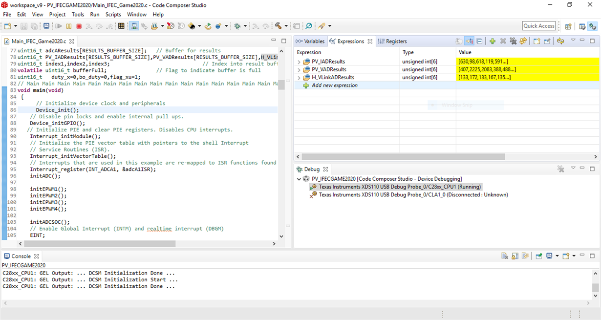
我和Green一起测试一下,结果如上
A1和C0分别是1V 100HZ和2V 50HZ的正弦信号
一、现象描述
280049 用的是 ADC 的A1 A2 和C0口 进行adc 转换 目前 A2和C0 转换都是正常的,但 A1的转换结果和C0 保持一致,不管这两个端口输入信号异同,A1的结果 同C0 ,C0 的结果是正确的。
触发是利用PWM1触发的,每次触发能连续转换这三路ADC 然后能进中断,读取信息。
二、程序代码
{/*
I_OUT as PV current output cpu_pin_9_A2 homologous 100pin as 9pin 64插脚
ADC_Vbus as PV Voltage cpu_pin_12_C0 homologous 100pin as 19pin 28插脚
ADC_Vlink as high bus voltage cpu_pin_14_A1 homologous 100pin as 22pin 30插脚
*/
// Setup VREF as internal
ADC_setVREF(ADCA_BASE, ADC_REFERENCE_INTERNAL, ADC_REFERENCE_3_3V);
ADC_setVREF(ADCC_BASE, ADC_REFERENCE_INTERNAL, ADC_REFERENCE_3_3V);
// Set ADCCLK divider to /4
ADC_setPrescaler(ADCA_BASE, ADC_CLK_DIV_4_0);
ADC_setPrescaler(ADCC_BASE, ADC_CLK_DIV_4_0);
// Set pulse positions to late
// ADC_setInterruptPulseMode(ADCA_BASE, ADC_PULSE_END_OF_CONV);
// ADC_setInterruptPulseMode(ADCC_BASE, ADC_PULSE_END_OF_CONV);
//ADC_disableContinuousMode(ADCA_BASE,ADC_INT_NUMBER1);
// 是ADC模块的基地址;socNumber是转换开始时的编号;触发将导致SOC的源;参数通道是与输入信号相关联的数字;sampleWindow是获取窗口的持续时间。
ADC_setupSOC(ADCA_BASE,ADC_SOC_NUMBER2, //ADC 需要转换的通道 PV_I
ADC_TRIGGER_EPWM1_SOCA, //ADC 触发
ADC_CH_ADCIN2, // A2 参数通道是与输入信号相关联的数字;
15); //Time
ADC_setupSOC(ADCC_BASE,ADC_SOC_NUMBER0, //ADC 需要转换的通道 PV_V
ADC_TRIGGER_EPWM1_SOCA, //ADC 触发
ADC_CH_ADCIN0, // C0 参数通道是与输入信号相关联的数字;
10); //转换 Time
ADC_setupSOC(ADCA_BASE, ADC_SOC_NUMBER1, //ADC 需要转换的通道 High_VBSU
ADC_TRIGGER_EPWM1_SOCA, //ADC 触发
ADC_CH_ADCIN1, // A1 参数通道是与输入信号相关联的数字;
24); //Time
// Power up the ADC and then delay for 1 ms
ADC_enableConverter(ADCA_BASE);
ADC_enableConverter(ADCC_BASE);
// DEVICE_DELAY_US(1000);
}
// initADCSOC – Function to configure ADCA's SOC0 to be triggered by ePWM1.
void initADCSOC(void)
{
// Configure burst mode for SOCs
ADC_enableBurstMode(ADCA_BASE);
ADC_setBurstModeConfig(ADCA_BASE, ADC_TRIGGER_EPWM1_SOCA,3);
// Set SOC0 to set the interrupt 1 flag. Enable the interrupt and make sure its flag is cleared.
ADC_setInterruptSource(ADCA_BASE, ADC_INT_NUMBER1, ADC_SOC_NUMBER1);//Set ADCA SOC1 to set the interrupt 1 flag
ADC_enableInterrupt(ADCA_BASE, ADC_INT_NUMBER1);
ADC_clearInterruptStatus(ADCA_BASE, ADC_INT_NUMBER1);
EPWM_enableADCTrigger(EPWM1_BASE, EPWM_SOC_A);//ENable ad trigger 选择PWM1 触发ADC
EPWM_setADCTriggerSource(EPWM1_BASE,EPWM_SOC_A,EPWM_SOC_TBCTR_ZERO);//时基计数器等于零
EPWM_setADCTriggerEventPrescale(EPWM1_BASE,EPWM_SOC_A,1);//为每个预分测单元生成SOC脉冲,多达15个事件
Interrupt_enable(INT_ADCA1);
}
// adcA1ISR – ADC A Interrupt 1 ISR
__interrupt void adcA1ISR(void)
{
/*
I_OUT as PV current output cpu_pin_9_A2 homologous 100pin as 9pin 64插脚
ADC_Vbus as PV Voltage cpu_pin_12_C0 homologous 100pin as 19pin 28插脚
ADC_Vlink as high bus voltage cpu_pin_14_A1 homologous 100pin as 22pin 30插脚
*/
// Add the latest result to the buffer resultBase是ADC结果的基地址 socNumber是转换开始时的编号
PV_IADResults[index1++] = ADC_readResult(ADCARESULT_BASE, ADC_SOC_NUMBER2);//A
PV_VADResults[index2++] = ADC_readResult(ADCCRESULT_BASE, ADC_SOC_NUMBER0);//A
H_VLinkADResults[index3++] = ADC_readResult(ADCARESULT_BASE, ADC_SOC_NUMBER8);//C
// Set the bufferFull flag if the buffer is full
if(RESULTS_BUFFER_SIZE <= index1)
{
index1 = 0;index2=0;index3=0;
bufferFull = 1;
}
// Clear the interrupt flag清除中断标志
ADC_clearInterruptStatus(ADCA_BASE, ADC_INT_NUMBER1);
// Check if overflow has occurred 检查是否发生溢出
if(true == ADC_getInterruptOverflowStatus(ADCA_BASE, ADC_INT_NUMBER1))
{
ADC_clearInterruptOverflowStatus(ADCA_BASE, ADC_INT_NUMBER1);
ADC_clearInterruptStatus(ADCA_BASE, ADC_INT_NUMBER1);
}
// Acknowledge the interrupt
Interrupt_clearACKGroup(INTERRUPT_ACK_GROUP1);
}
三、一直没有查出问题,硬件没有问题
njmail xu:
回复 Susan Yang:
Susan Yang你好! 你的测试说明我的程序没有问题? 为什么我这里测试和你的不一致呢?另有一问题,目前我用的280049的内部晶振,还是这个项目,如果提高PWM的精度,有什么方法,我是否已用到了最大的频率设置了。我自己认为最大了,大不确定,资料不清楚。
谢谢
一、现象描述
280049 用的是 ADC 的A1 A2 和C0口 进行adc 转换 目前 A2和C0 转换都是正常的,但 A1的转换结果和C0 保持一致,不管这两个端口输入信号异同,A1的结果 同C0 ,C0 的结果是正确的。
触发是利用PWM1触发的,每次触发能连续转换这三路ADC 然后能进中断,读取信息。
二、程序代码
{/*
I_OUT as PV current output cpu_pin_9_A2 homologous 100pin as 9pin 64插脚
ADC_Vbus as PV Voltage cpu_pin_12_C0 homologous 100pin as 19pin 28插脚
ADC_Vlink as high bus voltage cpu_pin_14_A1 homologous 100pin as 22pin 30插脚
*/
// Setup VREF as internal
ADC_setVREF(ADCA_BASE, ADC_REFERENCE_INTERNAL, ADC_REFERENCE_3_3V);
ADC_setVREF(ADCC_BASE, ADC_REFERENCE_INTERNAL, ADC_REFERENCE_3_3V);
// Set ADCCLK divider to /4
ADC_setPrescaler(ADCA_BASE, ADC_CLK_DIV_4_0);
ADC_setPrescaler(ADCC_BASE, ADC_CLK_DIV_4_0);
// Set pulse positions to late
// ADC_setInterruptPulseMode(ADCA_BASE, ADC_PULSE_END_OF_CONV);
// ADC_setInterruptPulseMode(ADCC_BASE, ADC_PULSE_END_OF_CONV);
//ADC_disableContinuousMode(ADCA_BASE,ADC_INT_NUMBER1);
// 是ADC模块的基地址;socNumber是转换开始时的编号;触发将导致SOC的源;参数通道是与输入信号相关联的数字;sampleWindow是获取窗口的持续时间。
ADC_setupSOC(ADCA_BASE,ADC_SOC_NUMBER2, //ADC 需要转换的通道 PV_I
ADC_TRIGGER_EPWM1_SOCA, //ADC 触发
ADC_CH_ADCIN2, // A2 参数通道是与输入信号相关联的数字;
15); //Time
ADC_setupSOC(ADCC_BASE,ADC_SOC_NUMBER0, //ADC 需要转换的通道 PV_V
ADC_TRIGGER_EPWM1_SOCA, //ADC 触发
ADC_CH_ADCIN0, // C0 参数通道是与输入信号相关联的数字;
10); //转换 Time
ADC_setupSOC(ADCA_BASE, ADC_SOC_NUMBER1, //ADC 需要转换的通道 High_VBSU
ADC_TRIGGER_EPWM1_SOCA, //ADC 触发
ADC_CH_ADCIN1, // A1 参数通道是与输入信号相关联的数字;
24); //Time
// Power up the ADC and then delay for 1 ms
ADC_enableConverter(ADCA_BASE);
ADC_enableConverter(ADCC_BASE);
// DEVICE_DELAY_US(1000);
}
// initADCSOC – Function to configure ADCA's SOC0 to be triggered by ePWM1.
void initADCSOC(void)
{
// Configure burst mode for SOCs
ADC_enableBurstMode(ADCA_BASE);
ADC_setBurstModeConfig(ADCA_BASE, ADC_TRIGGER_EPWM1_SOCA,3);
// Set SOC0 to set the interrupt 1 flag. Enable the interrupt and make sure its flag is cleared.
ADC_setInterruptSource(ADCA_BASE, ADC_INT_NUMBER1, ADC_SOC_NUMBER1);//Set ADCA SOC1 to set the interrupt 1 flag
ADC_enableInterrupt(ADCA_BASE, ADC_INT_NUMBER1);
ADC_clearInterruptStatus(ADCA_BASE, ADC_INT_NUMBER1);
EPWM_enableADCTrigger(EPWM1_BASE, EPWM_SOC_A);//ENable ad trigger 选择PWM1 触发ADC
EPWM_setADCTriggerSource(EPWM1_BASE,EPWM_SOC_A,EPWM_SOC_TBCTR_ZERO);//时基计数器等于零
EPWM_setADCTriggerEventPrescale(EPWM1_BASE,EPWM_SOC_A,1);//为每个预分测单元生成SOC脉冲,多达15个事件
Interrupt_enable(INT_ADCA1);
}
// adcA1ISR – ADC A Interrupt 1 ISR
__interrupt void adcA1ISR(void)
{
/*
I_OUT as PV current output cpu_pin_9_A2 homologous 100pin as 9pin 64插脚
ADC_Vbus as PV Voltage cpu_pin_12_C0 homologous 100pin as 19pin 28插脚
ADC_Vlink as high bus voltage cpu_pin_14_A1 homologous 100pin as 22pin 30插脚
*/
// Add the latest result to the buffer resultBase是ADC结果的基地址 socNumber是转换开始时的编号
PV_IADResults[index1++] = ADC_readResult(ADCARESULT_BASE, ADC_SOC_NUMBER2);//A
PV_VADResults[index2++] = ADC_readResult(ADCCRESULT_BASE, ADC_SOC_NUMBER0);//A
H_VLinkADResults[index3++] = ADC_readResult(ADCARESULT_BASE, ADC_SOC_NUMBER8);//C
// Set the bufferFull flag if the buffer is full
if(RESULTS_BUFFER_SIZE <= index1)
{
index1 = 0;index2=0;index3=0;
bufferFull = 1;
}
// Clear the interrupt flag清除中断标志
ADC_clearInterruptStatus(ADCA_BASE, ADC_INT_NUMBER1);
// Check if overflow has occurred 检查是否发生溢出
if(true == ADC_getInterruptOverflowStatus(ADCA_BASE, ADC_INT_NUMBER1))
{
ADC_clearInterruptOverflowStatus(ADCA_BASE, ADC_INT_NUMBER1);
ADC_clearInterruptStatus(ADCA_BASE, ADC_INT_NUMBER1);
}
// Acknowledge the interrupt
Interrupt_clearACKGroup(INTERRUPT_ACK_GROUP1);
}
三、一直没有查出问题,硬件没有问题
njmail xu:
回复 njmail xu:
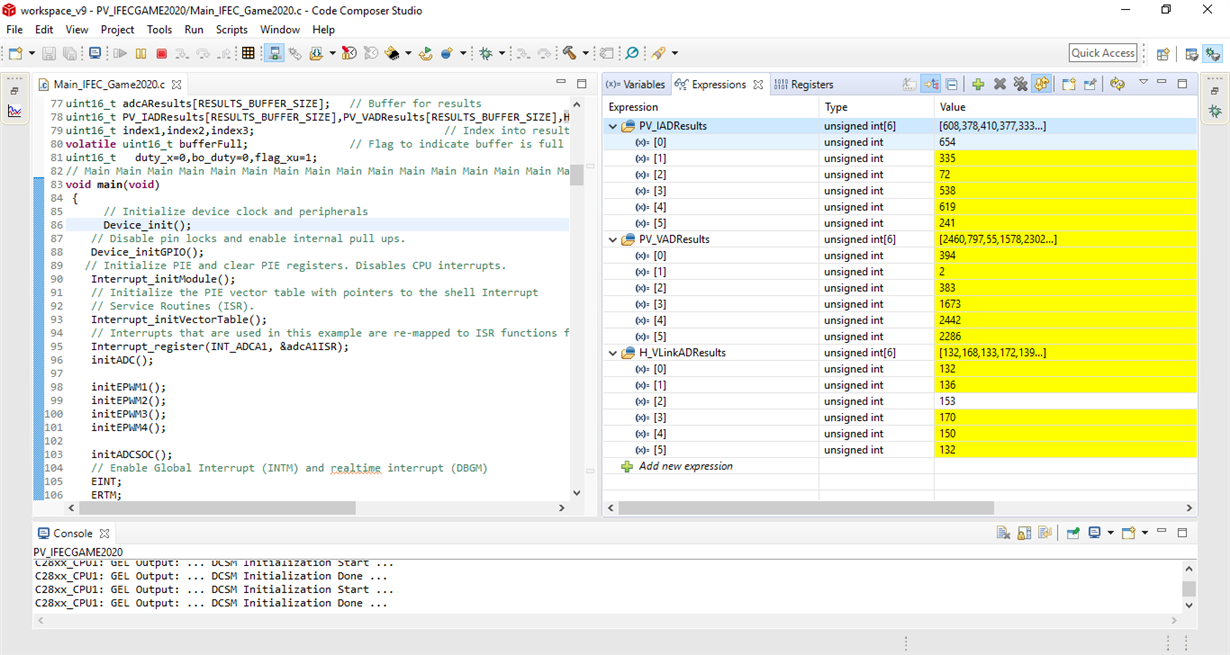
为什么我仿真的结果和你们不一样呢?你们修改了那个地方? 后面2个数组数据完全一样 ?
一、现象描述
280049 用的是 ADC 的A1 A2 和C0口 进行adc 转换 目前 A2和C0 转换都是正常的,但 A1的转换结果和C0 保持一致,不管这两个端口输入信号异同,A1的结果 同C0 ,C0 的结果是正确的。
触发是利用PWM1触发的,每次触发能连续转换这三路ADC 然后能进中断,读取信息。
二、程序代码
{/*
I_OUT as PV current output cpu_pin_9_A2 homologous 100pin as 9pin 64插脚
ADC_Vbus as PV Voltage cpu_pin_12_C0 homologous 100pin as 19pin 28插脚
ADC_Vlink as high bus voltage cpu_pin_14_A1 homologous 100pin as 22pin 30插脚
*/
// Setup VREF as internal
ADC_setVREF(ADCA_BASE, ADC_REFERENCE_INTERNAL, ADC_REFERENCE_3_3V);
ADC_setVREF(ADCC_BASE, ADC_REFERENCE_INTERNAL, ADC_REFERENCE_3_3V);
// Set ADCCLK divider to /4
ADC_setPrescaler(ADCA_BASE, ADC_CLK_DIV_4_0);
ADC_setPrescaler(ADCC_BASE, ADC_CLK_DIV_4_0);
// Set pulse positions to late
// ADC_setInterruptPulseMode(ADCA_BASE, ADC_PULSE_END_OF_CONV);
// ADC_setInterruptPulseMode(ADCC_BASE, ADC_PULSE_END_OF_CONV);
//ADC_disableContinuousMode(ADCA_BASE,ADC_INT_NUMBER1);
// 是ADC模块的基地址;socNumber是转换开始时的编号;触发将导致SOC的源;参数通道是与输入信号相关联的数字;sampleWindow是获取窗口的持续时间。
ADC_setupSOC(ADCA_BASE,ADC_SOC_NUMBER2, //ADC 需要转换的通道 PV_I
ADC_TRIGGER_EPWM1_SOCA, //ADC 触发
ADC_CH_ADCIN2, // A2 参数通道是与输入信号相关联的数字;
15); //Time
ADC_setupSOC(ADCC_BASE,ADC_SOC_NUMBER0, //ADC 需要转换的通道 PV_V
ADC_TRIGGER_EPWM1_SOCA, //ADC 触发
ADC_CH_ADCIN0, // C0 参数通道是与输入信号相关联的数字;
10); //转换 Time
ADC_setupSOC(ADCA_BASE, ADC_SOC_NUMBER1, //ADC 需要转换的通道 High_VBSU
ADC_TRIGGER_EPWM1_SOCA, //ADC 触发
ADC_CH_ADCIN1, // A1 参数通道是与输入信号相关联的数字;
24); //Time
// Power up the ADC and then delay for 1 ms
ADC_enableConverter(ADCA_BASE);
ADC_enableConverter(ADCC_BASE);
// DEVICE_DELAY_US(1000);
}
// initADCSOC – Function to configure ADCA's SOC0 to be triggered by ePWM1.
void initADCSOC(void)
{
// Configure burst mode for SOCs
ADC_enableBurstMode(ADCA_BASE);
ADC_setBurstModeConfig(ADCA_BASE, ADC_TRIGGER_EPWM1_SOCA,3);
// Set SOC0 to set the interrupt 1 flag. Enable the interrupt and make sure its flag is cleared.
ADC_setInterruptSource(ADCA_BASE, ADC_INT_NUMBER1, ADC_SOC_NUMBER1);//Set ADCA SOC1 to set the interrupt 1 flag
ADC_enableInterrupt(ADCA_BASE, ADC_INT_NUMBER1);
ADC_clearInterruptStatus(ADCA_BASE, ADC_INT_NUMBER1);
EPWM_enableADCTrigger(EPWM1_BASE, EPWM_SOC_A);//ENable ad trigger 选择PWM1 触发ADC
EPWM_setADCTriggerSource(EPWM1_BASE,EPWM_SOC_A,EPWM_SOC_TBCTR_ZERO);//时基计数器等于零
EPWM_setADCTriggerEventPrescale(EPWM1_BASE,EPWM_SOC_A,1);//为每个预分测单元生成SOC脉冲,多达15个事件
Interrupt_enable(INT_ADCA1);
}
// adcA1ISR – ADC A Interrupt 1 ISR
__interrupt void adcA1ISR(void)
{
/*
I_OUT as PV current output cpu_pin_9_A2 homologous 100pin as 9pin 64插脚
ADC_Vbus as PV Voltage cpu_pin_12_C0 homologous 100pin as 19pin 28插脚
ADC_Vlink as high bus voltage cpu_pin_14_A1 homologous 100pin as 22pin 30插脚
*/
// Add the latest result to the buffer resultBase是ADC结果的基地址 socNumber是转换开始时的编号
PV_IADResults[index1++] = ADC_readResult(ADCARESULT_BASE, ADC_SOC_NUMBER2);//A
PV_VADResults[index2++] = ADC_readResult(ADCCRESULT_BASE, ADC_SOC_NUMBER0);//A
H_VLinkADResults[index3++] = ADC_readResult(ADCARESULT_BASE, ADC_SOC_NUMBER8);//C
// Set the bufferFull flag if the buffer is full
if(RESULTS_BUFFER_SIZE <= index1)
{
index1 = 0;index2=0;index3=0;
bufferFull = 1;
}
// Clear the interrupt flag清除中断标志
ADC_clearInterruptStatus(ADCA_BASE, ADC_INT_NUMBER1);
// Check if overflow has occurred 检查是否发生溢出
if(true == ADC_getInterruptOverflowStatus(ADCA_BASE, ADC_INT_NUMBER1))
{
ADC_clearInterruptOverflowStatus(ADCA_BASE, ADC_INT_NUMBER1);
ADC_clearInterruptStatus(ADCA_BASE, ADC_INT_NUMBER1);
}
// Acknowledge the interrupt
Interrupt_clearACKGroup(INTERRUPT_ACK_GROUP1);
}
三、一直没有查出问题,硬件没有问题
Susan Yang:
回复 njmail xu:
很抱歉,您的图片无法显示
我们没有对您的代码进行任何修改
使用的是CCS 9.0
一、现象描述
280049 用的是 ADC 的A1 A2 和C0口 进行adc 转换 目前 A2和C0 转换都是正常的,但 A1的转换结果和C0 保持一致,不管这两个端口输入信号异同,A1的结果 同C0 ,C0 的结果是正确的。
触发是利用PWM1触发的,每次触发能连续转换这三路ADC 然后能进中断,读取信息。
二、程序代码
{/*
I_OUT as PV current output cpu_pin_9_A2 homologous 100pin as 9pin 64插脚
ADC_Vbus as PV Voltage cpu_pin_12_C0 homologous 100pin as 19pin 28插脚
ADC_Vlink as high bus voltage cpu_pin_14_A1 homologous 100pin as 22pin 30插脚
*/
// Setup VREF as internal
ADC_setVREF(ADCA_BASE, ADC_REFERENCE_INTERNAL, ADC_REFERENCE_3_3V);
ADC_setVREF(ADCC_BASE, ADC_REFERENCE_INTERNAL, ADC_REFERENCE_3_3V);
// Set ADCCLK divider to /4
ADC_setPrescaler(ADCA_BASE, ADC_CLK_DIV_4_0);
ADC_setPrescaler(ADCC_BASE, ADC_CLK_DIV_4_0);
// Set pulse positions to late
// ADC_setInterruptPulseMode(ADCA_BASE, ADC_PULSE_END_OF_CONV);
// ADC_setInterruptPulseMode(ADCC_BASE, ADC_PULSE_END_OF_CONV);
//ADC_disableContinuousMode(ADCA_BASE,ADC_INT_NUMBER1);
// 是ADC模块的基地址;socNumber是转换开始时的编号;触发将导致SOC的源;参数通道是与输入信号相关联的数字;sampleWindow是获取窗口的持续时间。
ADC_setupSOC(ADCA_BASE,ADC_SOC_NUMBER2, //ADC 需要转换的通道 PV_I
ADC_TRIGGER_EPWM1_SOCA, //ADC 触发
ADC_CH_ADCIN2, // A2 参数通道是与输入信号相关联的数字;
15); //Time
ADC_setupSOC(ADCC_BASE,ADC_SOC_NUMBER0, //ADC 需要转换的通道 PV_V
ADC_TRIGGER_EPWM1_SOCA, //ADC 触发
ADC_CH_ADCIN0, // C0 参数通道是与输入信号相关联的数字;
10); //转换 Time
ADC_setupSOC(ADCA_BASE, ADC_SOC_NUMBER1, //ADC 需要转换的通道 High_VBSU
ADC_TRIGGER_EPWM1_SOCA, //ADC 触发
ADC_CH_ADCIN1, // A1 参数通道是与输入信号相关联的数字;
24); //Time
// Power up the ADC and then delay for 1 ms
ADC_enableConverter(ADCA_BASE);
ADC_enableConverter(ADCC_BASE);
// DEVICE_DELAY_US(1000);
}
// initADCSOC – Function to configure ADCA's SOC0 to be triggered by ePWM1.
void initADCSOC(void)
{
// Configure burst mode for SOCs
ADC_enableBurstMode(ADCA_BASE);
ADC_setBurstModeConfig(ADCA_BASE, ADC_TRIGGER_EPWM1_SOCA,3);
// Set SOC0 to set the interrupt 1 flag. Enable the interrupt and make sure its flag is cleared.
ADC_setInterruptSource(ADCA_BASE, ADC_INT_NUMBER1, ADC_SOC_NUMBER1);//Set ADCA SOC1 to set the interrupt 1 flag
ADC_enableInterrupt(ADCA_BASE, ADC_INT_NUMBER1);
ADC_clearInterruptStatus(ADCA_BASE, ADC_INT_NUMBER1);
EPWM_enableADCTrigger(EPWM1_BASE, EPWM_SOC_A);//ENable ad trigger 选择PWM1 触发ADC
EPWM_setADCTriggerSource(EPWM1_BASE,EPWM_SOC_A,EPWM_SOC_TBCTR_ZERO);//时基计数器等于零
EPWM_setADCTriggerEventPrescale(EPWM1_BASE,EPWM_SOC_A,1);//为每个预分测单元生成SOC脉冲,多达15个事件
Interrupt_enable(INT_ADCA1);
}
// adcA1ISR – ADC A Interrupt 1 ISR
__interrupt void adcA1ISR(void)
{
/*
I_OUT as PV current output cpu_pin_9_A2 homologous 100pin as 9pin 64插脚
ADC_Vbus as PV Voltage cpu_pin_12_C0 homologous 100pin as 19pin 28插脚
ADC_Vlink as high bus voltage cpu_pin_14_A1 homologous 100pin as 22pin 30插脚
*/
// Add the latest result to the buffer resultBase是ADC结果的基地址 socNumber是转换开始时的编号
PV_IADResults[index1++] = ADC_readResult(ADCARESULT_BASE, ADC_SOC_NUMBER2);//A
PV_VADResults[index2++] = ADC_readResult(ADCCRESULT_BASE, ADC_SOC_NUMBER0);//A
H_VLinkADResults[index3++] = ADC_readResult(ADCARESULT_BASE, ADC_SOC_NUMBER8);//C
// Set the bufferFull flag if the buffer is full
if(RESULTS_BUFFER_SIZE <= index1)
{
index1 = 0;index2=0;index3=0;
bufferFull = 1;
}
// Clear the interrupt flag清除中断标志
ADC_clearInterruptStatus(ADCA_BASE, ADC_INT_NUMBER1);
// Check if overflow has occurred 检查是否发生溢出
if(true == ADC_getInterruptOverflowStatus(ADCA_BASE, ADC_INT_NUMBER1))
{
ADC_clearInterruptOverflowStatus(ADCA_BASE, ADC_INT_NUMBER1);
ADC_clearInterruptStatus(ADCA_BASE, ADC_INT_NUMBER1);
}
// Acknowledge the interrupt
Interrupt_clearACKGroup(INTERRUPT_ACK_GROUP1);
}
三、一直没有查出问题,硬件没有问题
njmail xu:
回复 Susan Yang:
一、现象描述
280049 用的是 ADC 的A1 A2 和C0口 进行adc 转换 目前 A2和C0 转换都是正常的,但 A1的转换结果和C0 保持一致,不管这两个端口输入信号异同,A1的结果 同C0 ,C0 的结果是正确的。
触发是利用PWM1触发的,每次触发能连续转换这三路ADC 然后能进中断,读取信息。
二、程序代码
{/*
I_OUT as PV current output cpu_pin_9_A2 homologous 100pin as 9pin 64插脚
ADC_Vbus as PV Voltage cpu_pin_12_C0 homologous 100pin as 19pin 28插脚
ADC_Vlink as high bus voltage cpu_pin_14_A1 homologous 100pin as 22pin 30插脚
*/
// Setup VREF as internal
ADC_setVREF(ADCA_BASE, ADC_REFERENCE_INTERNAL, ADC_REFERENCE_3_3V);
ADC_setVREF(ADCC_BASE, ADC_REFERENCE_INTERNAL, ADC_REFERENCE_3_3V);
// Set ADCCLK divider to /4
ADC_setPrescaler(ADCA_BASE, ADC_CLK_DIV_4_0);
ADC_setPrescaler(ADCC_BASE, ADC_CLK_DIV_4_0);
// Set pulse positions to late
// ADC_setInterruptPulseMode(ADCA_BASE, ADC_PULSE_END_OF_CONV);
// ADC_setInterruptPulseMode(ADCC_BASE, ADC_PULSE_END_OF_CONV);
//ADC_disableContinuousMode(ADCA_BASE,ADC_INT_NUMBER1);
// 是ADC模块的基地址;socNumber是转换开始时的编号;触发将导致SOC的源;参数通道是与输入信号相关联的数字;sampleWindow是获取窗口的持续时间。
ADC_setupSOC(ADCA_BASE,ADC_SOC_NUMBER2, //ADC 需要转换的通道 PV_I
ADC_TRIGGER_EPWM1_SOCA, //ADC 触发
ADC_CH_ADCIN2, // A2 参数通道是与输入信号相关联的数字;
15); //Time
ADC_setupSOC(ADCC_BASE,ADC_SOC_NUMBER0, //ADC 需要转换的通道 PV_V
ADC_TRIGGER_EPWM1_SOCA, //ADC 触发
ADC_CH_ADCIN0, // C0 参数通道是与输入信号相关联的数字;
10); //转换 Time
ADC_setupSOC(ADCA_BASE, ADC_SOC_NUMBER1, //ADC 需要转换的通道 High_VBSU
ADC_TRIGGER_EPWM1_SOCA, //ADC 触发
ADC_CH_ADCIN1, // A1 参数通道是与输入信号相关联的数字;
24); //Time
// Power up the ADC and then delay for 1 ms
ADC_enableConverter(ADCA_BASE);
ADC_enableConverter(ADCC_BASE);
// DEVICE_DELAY_US(1000);
}
// initADCSOC – Function to configure ADCA's SOC0 to be triggered by ePWM1.
void initADCSOC(void)
{
// Configure burst mode for SOCs
ADC_enableBurstMode(ADCA_BASE);
ADC_setBurstModeConfig(ADCA_BASE, ADC_TRIGGER_EPWM1_SOCA,3);
// Set SOC0 to set the interrupt 1 flag. Enable the interrupt and make sure its flag is cleared.
ADC_setInterruptSource(ADCA_BASE, ADC_INT_NUMBER1, ADC_SOC_NUMBER1);//Set ADCA SOC1 to set the interrupt 1 flag
ADC_enableInterrupt(ADCA_BASE, ADC_INT_NUMBER1);
ADC_clearInterruptStatus(ADCA_BASE, ADC_INT_NUMBER1);
EPWM_enableADCTrigger(EPWM1_BASE, EPWM_SOC_A);//ENable ad trigger 选择PWM1 触发ADC
EPWM_setADCTriggerSource(EPWM1_BASE,EPWM_SOC_A,EPWM_SOC_TBCTR_ZERO);//时基计数器等于零
EPWM_setADCTriggerEventPrescale(EPWM1_BASE,EPWM_SOC_A,1);//为每个预分测单元生成SOC脉冲,多达15个事件
Interrupt_enable(INT_ADCA1);
}
// adcA1ISR – ADC A Interrupt 1 ISR
__interrupt void adcA1ISR(void)
{
/*
I_OUT as PV current output cpu_pin_9_A2 homologous 100pin as 9pin 64插脚
ADC_Vbus as PV Voltage cpu_pin_12_C0 homologous 100pin as 19pin 28插脚
ADC_Vlink as high bus voltage cpu_pin_14_A1 homologous 100pin as 22pin 30插脚
*/
// Add the latest result to the buffer resultBase是ADC结果的基地址 socNumber是转换开始时的编号
PV_IADResults[index1++] = ADC_readResult(ADCARESULT_BASE, ADC_SOC_NUMBER2);//A
PV_VADResults[index2++] = ADC_readResult(ADCCRESULT_BASE, ADC_SOC_NUMBER0);//A
H_VLinkADResults[index3++] = ADC_readResult(ADCARESULT_BASE, ADC_SOC_NUMBER8);//C
// Set the bufferFull flag if the buffer is full
if(RESULTS_BUFFER_SIZE <= index1)
{
index1 = 0;index2=0;index3=0;
bufferFull = 1;
}
// Clear the interrupt flag清除中断标志
ADC_clearInterruptStatus(ADCA_BASE, ADC_INT_NUMBER1);
// Check if overflow has occurred 检查是否发生溢出
if(true == ADC_getInterruptOverflowStatus(ADCA_BASE, ADC_INT_NUMBER1))
{
ADC_clearInterruptOverflowStatus(ADCA_BASE, ADC_INT_NUMBER1);
ADC_clearInterruptStatus(ADCA_BASE, ADC_INT_NUMBER1);
}
// Acknowledge the interrupt
Interrupt_clearACKGroup(INTERRUPT_ACK_GROUP1);
}
三、一直没有查出问题,硬件没有问题
njmail xu:
回复 njmail xu:
我用的是ccs9.3为什么我这里测试和你的不一致呢?
另有一问题,目前我用的280049的内部晶振,还是这个项目,如果提高PWM的精度,有什么方法,我是否已用到了最大的频率设置了。我自己认为最大了,大不确定,资料不清楚。


