我用的开发板是Digitally Controlled Solar Micro Inverter Design using C2000 Piccolo Microcontroller 。
在进行DCDC部分MPPT闭环实验时,变压器会发出响声而且持续一会后电路断开,EPWM3故障标志显示过流保护,但我设置的光伏开路电压38V,短路电流1.5A,实际电流最高也就限制在1.5A 。 为什么会发生过流保护呢?我看程序中电流限制是10A 。还有SolarMicroInv-Main.c中的保护程序里COMP3的输入电压a在哪里配置呢?我在SolarMicroInv-DevInit_F2803x.c、SolarMicroInv-Settings.h、SolarMicroInv-Includes.h中都没有找到。
谢谢大家!
保护代码如下:
/********* Protection Mechanisms *****************/
//TODO Protection Code
EALLOW;
//TODO Protection Code
EALLOW;
// Cycle by cycle interrupt for CPU halt trip
EPwm1Regs.TZSEL.bit.CBC6 = 0x1;
EPwm2Regs.TZSEL.bit.CBC6 = 0x1;
EPwm3Regs.TZSEL.bit.CBC6 = 0x1;
EPwm1Regs.TZSEL.bit.CBC6 = 0x1;
EPwm2Regs.TZSEL.bit.CBC6 = 0x1;
EPwm3Regs.TZSEL.bit.CBC6 = 0x1;
// Adding one shot trip for over-current protection on the inverter TZ2
EPwm1Regs.TZSEL.bit.OSHT2 = 0x1;
EPwm2Regs.TZSEL.bit.OSHT2 = 0x1;
EPwm1Regs.TZSEL.bit.OSHT2 = 0x1;
EPwm2Regs.TZSEL.bit.OSHT2 = 0x1;
// Adding one shot trip for over current of the flyback stage but avoid the <1% duty condition using blanking
// First enable the COMP3
Comp3Regs.COMPCTL.bit.COMPDACEN =0x1;
Comp3Regs.COMPCTL.bit.SYNCSEL =0x0; // asynchronous version of the COMP signal is passed to the EPWM/GPIO module
Comp3Regs.COMPCTL.bit.CMPINV =0x0; // Output of the comparator is passed directly
Comp3Regs.COMPCTL.bit.COMPSOURCE =0x0; // inverting input of the comparator is connected to the internal DAC
Comp3Regs.DACVAL.bit.DACVAL =700; // set DAC input to peak trip point ~10 Amps, full scale is 15Amps
AdcRegs.COMPHYSTCTL.bit.COMP1_HYST_DISABLE = 0x1;
//Select COMP3 as one shot trip
EPwm3Regs.DCTRIPSEL.bit.DCAHCOMPSEL=DC_COMP3OUT ;
EPwm3Regs.TZDCSEL.bit.DCAEVT1=TZ_DCAH_HI;
EPwm3Regs.DCACTL.bit.EVT1SRCSEL = DC_EVT_FLT ;
EPwm3Regs.DCACTL.bit.EVT1FRCSYNCSEL=DC_EVT_ASYNC;
EPwm3Regs.TZSEL.bit.DCAEVT1=0x1;
EPwm3Regs.DCTRIPSEL.bit.DCAHCOMPSEL=DC_COMP3OUT ;
EPwm3Regs.TZDCSEL.bit.DCAEVT1=TZ_DCAH_HI;
EPwm3Regs.DCACTL.bit.EVT1SRCSEL = DC_EVT_FLT ;
EPwm3Regs.DCACTL.bit.EVT1FRCSYNCSEL=DC_EVT_ASYNC;
EPwm3Regs.TZSEL.bit.DCAEVT1=0x1;
//Add blanking to avoid conditions where the over current trip generates <1% duty cycle
EPwm3Regs.DCFCTL.bit.BLANKE=DC_BLANK_ENABLE; // Blanking window is enabled
EPwm3Regs.DCFCTL.bit.BLANKINV=DC_BLANK_NOTINV; // Blanking window is not inverted
EPwm3Regs.DCFCTL.bit.SRCSEL=DC_SRC_DCAEVT1; //DCAEVT1
EPwm3Regs.DCFCTL.bit.PULSESEL=DC_PULSESEL_PRD; // apply offset from TBCTR=TBPRD
EPwm3Regs.DCFOFFSET=59;
EPwm3Regs.DCFWINDOW=255;
EPwm3Regs.DCFCTL.bit.BLANKINV=DC_BLANK_NOTINV; // Blanking window is not inverted
EPwm3Regs.DCFCTL.bit.SRCSEL=DC_SRC_DCAEVT1; //DCAEVT1
EPwm3Regs.DCFCTL.bit.PULSESEL=DC_PULSESEL_PRD; // apply offset from TBCTR=TBPRD
EPwm3Regs.DCFOFFSET=59;
EPwm3Regs.DCFWINDOW=255;
// What do we want the OST/CBC events to do?
// TZA events can force EPWMxA
// TZB events can force EPWMxB
// TZA events can force EPWMxA
// TZB events can force EPWMxB
EPwm1Regs.TZCTL.bit.TZA = TZ_FORCE_LO; // EPWMxA will go low
EPwm1Regs.TZCTL.bit.TZB = TZ_FORCE_LO; // EPWMxB will go low
EPwm1Regs.TZCTL.bit.TZB = TZ_FORCE_LO; // EPWMxB will go low
EPwm2Regs.TZCTL.bit.TZA = TZ_FORCE_LO; // EPWMxA will go low
EPwm2Regs.TZCTL.bit.TZB = TZ_FORCE_LO; // EPWMxB will go low
EPwm2Regs.TZCTL.bit.TZB = TZ_FORCE_LO; // EPWMxB will go low
EPwm3Regs.TZCTL.bit.TZA = TZ_FORCE_LO; // EPWMxA will go low
EPwm3Regs.TZCTL.bit.TZB = TZ_FORCE_LO; // EPWMxB will go low
EPwm3Regs.TZCTL.bit.TZB = TZ_FORCE_LO; // EPWMxB will go low
//clear any spurious trips
EPwm1Regs.TZCLR.bit.OST = 1;
EPwm2Regs.TZCLR.bit.OST = 1;
EPwm3Regs.TZCLR.bit.OST = 1;
EPwm1Regs.TZCLR.bit.OST = 1;
EPwm2Regs.TZCLR.bit.OST = 1;
EPwm3Regs.TZCLR.bit.OST = 1;
// Force a trip event on all the PWM modules for safety
EPwm1Regs.TZFRC.bit.OST = 0x1;
EPwm2Regs.TZFRC.bit.OST = 0x1;
EPwm3Regs.TZFRC.bit.OST = 0x1;
EDIS;
EPwm1Regs.TZFRC.bit.OST = 0x1;
EPwm2Regs.TZFRC.bit.OST = 0x1;
EPwm3Regs.TZFRC.bit.OST = 0x1;
EDIS;
/********* Protection Mechanism END *****************/
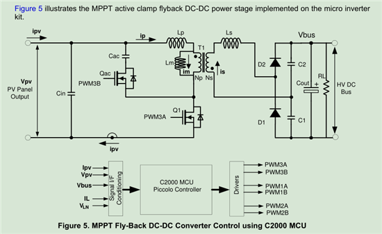
下图是DCDC部分原理图
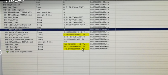
下图为故障发生后参数界面 可以看到倒数第四行EPWM3Regs.TZFLG.all=12,而且故障时倒数第八行占空比达到了0.8,duty_flyback_pu=0.8
Xiangjie Kong:
回复 Rayna Wang:
感谢您的耐心回复!按照您提供的第二个思路已经找到问题发生的原因。非常感谢!