我想烧写程序到2812的flash里,程序里带有IQMATH.LIB
cmd文件如下,是用ezdsp的cmd文件修改一下得到的。
请问为什么DSP掉电后依然不能从flash里运行
/*
// TI File $Revision: /main/2 $
// Checkin $Date: April 28, 2005 15:19:56 $
//###########################################################################
//
// FILE: F2812.cmd
//
// TITLE: Linker Command File For F2812 Device
//
//###########################################################################
// $TI Release: DSP281x C/C++ Header Files V1.20 $
// $Release Date: July 27, 2009 $
//###########################################################################
*/
/* ======================================================
// For Code Composer Studio V2.2 and later
// —————————————
// In addition to this memory linker command file,// add the header linker command file directly to the project.// The header linker command file is required to link the
// peripheral structures to the proper locations within// the memory map.
//
// The header linker files are found in <base>\DSP281x_Headers\cmd
//// For BIOS applications add: DSP281x_Headers_nonBIOS.cmd
// For nonBIOS applications add: DSP281x_Headers_nonBIOS.cmd========================================================= */
/* ======================================================
// For Code Composer Studio prior to V2.2
// ————————————–
// 1) Use one of the following -l statements to include the// header linker command file in the project. The header linker
// file is required to link the peripheral structures to the proper// locations within the memory map */
/* Uncomment this line to include file only for non-BIOS applications */
/* -l DSP281x_Headers_nonBIOS.cmd */
/* Uncomment this line to include file only for BIOS applications */
/* -l DSP281x_Headers_BIOS.cmd */
/* 2) In your project add the path to <base>\DSP281x_headers\cmd to the
library search path under project->build options, linker tab, library search path (-i).
/*========================================================= */
/* Define the memory block start/length for the F2812 PAGE 0 will be used to organize program sections
PAGE 1 will be used to organize data sections
Notes: Memory blocks on F2812 are uniform (ie same
physical memory) in both PAGE 0 and PAGE 1. That is the same memory region should not be
defined for both PAGE 0 and PAGE 1.
Doing so will result in corruption of program and/or data.*/
MEMORY
{
PAGE 0: /* Program Memory */
/* Memory (RAM/FLASH/OTP) blocks can be moved to PAGE1 for data allocation */
ZONE0 : origin = 0x002000, length = 0x002000 /* XINTF zone 0 */
ZONE1 : origin = 0x004000, length = 0x002000 /* XINTF zone 1 */
RAML0 : origin = 0x008000, length = 0x001000 /* on-chip RAM block L0 */
ZONE2 : origin = 0x080000, length = 0x080000 /* XINTF zone 2 */
ZONE6 : origin = 0x100000, length = 0x080000 /* XINTF zone 6 */
OTP : origin = 0x3D7800, length = 0x000800 /* on-chip OTP */
FLASHJ : origin = 0x3D8000, length = 0x002000 /* on-chip FLASH */
FLASHI : origin = 0x3DA000, length = 0x002000 /* on-chip FLASH */
FLASHH : origin = 0x3DC000, length = 0x004000 /* on-chip FLASH */
FLASHG : origin = 0x3E0000, length = 0x004000 /* on-chip FLASH */
FLASHF : origin = 0x3E4000, length = 0x004000 /* on-chip FLASH */
FLASHE : origin = 0x3E8000, length = 0x004000 /* on-chip FLASH */
FLASHD : origin = 0x3EC000, length = 0x004000 /* on-chip FLASH */
FLASHC : origin = 0x3F0000, length = 0x004000 /* on-chip FLASH */
FLASHA : origin = 0x3F6000, length = 0x001F80 /* on-chip FLASH */
CSM_RSVD : origin = 0x3F7F80, length = 0x000076 /* Part of FLASHA. Program with all 0x0000 when CSM is in use. */
BEGIN : origin = 0x3F7FF6, length = 0x000002 /* Part of FLASHA. Used for "boot to Flash" bootloader mode. */
CSM_PWL : origin = 0x3F7FF8, length = 0x000008 /* Part of FLASHA. CSM password locations in FLASHA */
/* ZONE7 : origin = 0x3FC000, length = 0x003FC0 /* XINTF zone 7 available if MP/MCn=1 */// ROM : origin = 0x3FF000, length = 0x000FC0 /* Boot ROM available if MP/MCn=0 */ //?为了q格式把此行注释掉,不知是否有隐患
RESET : origin = 0x3FFFC0, length = 0x000002 /* part of boot ROM (MP/MCn=0) or XINTF zone 7 (MP/MCn=1) */
VECTORS : origin = 0x3FFFC2, length = 0x00003E /* part of boot ROM (MP/MCn=0) or XINTF zone 7 (MP/MCn=1) */
BOOTROM (RW) : origin = 0x3ff000, length = 0x000fc0 //用于加入库函数存储Q格式相关函数
RAMH0 (RW) : origin = 0x3f8000, length = 0x002000 //用于加入库函数存储Q格式
PAGE 1 : /* Data Memory */
/* Memory (RAM/FLASH/OTP) blocks can be moved to PAGE0 for program allocation */
/* Registers remain on PAGE1 */
RAMM0 : origin = 0x000000, length = 0x000400 /* on-chip RAM block M0 */
RAMM1 : origin = 0x000400, length = 0x000400 /* on-chip RAM block M1 */
RAML1 : origin = 0x009000, length = 0x001000 /* on-chip RAM block L1 */
FLASHB : origin = 0x3F4000, length = 0x002000 /* on-chip FLASH */
RAMH0 : origin = 0x3F8000, length = 0x002000 /* on-chip RAM block H0 */
}
/* Allocate sections to memory blocks.
Note:
codestart user defined section in DSP28_CodeStartBranch.asm used to redirect code execution when booting to flash
ramfuncs user defined section to store functions that will be copied from Flash into RAM
*/SECTIONS
{
/* Allocate program areas: */
.cinit : > FLASHA PAGE = 0
.pinit : > FLASHA, PAGE = 0
.text : > FLASHA PAGE = 0
codestart : > BEGIN PAGE = 0
ramfuncs : LOAD = FLASHD, RUN = RAML0, LOAD_START(_RamfuncsLoadStart),
LOAD_END(_RamfuncsLoadEnd),
RUN_START(_RamfuncsRunStart),
PAGE = 0
csmpasswds : > CSM_PWL PAGE = 0
csm_rsvd : > CSM_RSVD PAGE = 0
/* Allocate uninitalized data sections: */
.stack : > RAMM0 PAGE = 1
.ebss : > RAML1 PAGE = 1
.esysmem : > RAMH0 PAGE = 1
/* Initalized sections go in Flash */
/* For SDFlash to program these, they must be allocated to page 0 */
.econst : > FLASHA PAGE = 0
.switch : > FLASHA PAGE = 0
/* Allocate IQ math areas: */
// IQmath : > FLASHC PAGE = 0 /* Math Code */ //?为了q格式把此行注释掉,不知是否有隐患
// IQmathTables : > ROM PAGE = 0, TYPE = NOLOAD /* Math Tables In ROM */ //?为了q格式把此行注释掉,不知是否有隐患
/* .reset is a standard section used by the compiler. It contains the */ /* the address of the start of _c_int00 for C Code. /*
/* When using the boot ROM this section and the CPU vector */
/* table is not needed. Thus the default type is set here to */
/* DSECT */ .reset : > RESET, PAGE = 0, TYPE = DSECT
vectors : > VECTORS PAGE = 0, TYPE = DSECT
IQmathTables : load = BOOTROM, type = NOLOAD, PAGE = 0 //用于加入库函数存储Q格式相关函数
IQmath : load = RAMH0, PAGE = 0 //用于加入库函数存储Q格式相关函数
}
Seven Han:
请问您用的是ti的evm板吗还是自己设计的板子呢?
我想烧写程序到2812的flash里,程序里带有IQMATH.LIB
cmd文件如下,是用ezdsp的cmd文件修改一下得到的。
请问为什么DSP掉电后依然不能从flash里运行
/*
// TI File $Revision: /main/2 $
// Checkin $Date: April 28, 2005 15:19:56 $
//###########################################################################
//
// FILE: F2812.cmd
//
// TITLE: Linker Command File For F2812 Device
//
//###########################################################################
// $TI Release: DSP281x C/C++ Header Files V1.20 $
// $Release Date: July 27, 2009 $
//###########################################################################
*/
/* ======================================================
// For Code Composer Studio V2.2 and later
// —————————————
// In addition to this memory linker command file,// add the header linker command file directly to the project.// The header linker command file is required to link the
// peripheral structures to the proper locations within// the memory map.
//
// The header linker files are found in <base>\DSP281x_Headers\cmd
//// For BIOS applications add: DSP281x_Headers_nonBIOS.cmd
// For nonBIOS applications add: DSP281x_Headers_nonBIOS.cmd========================================================= */
/* ======================================================
// For Code Composer Studio prior to V2.2
// ————————————–
// 1) Use one of the following -l statements to include the// header linker command file in the project. The header linker
// file is required to link the peripheral structures to the proper// locations within the memory map */
/* Uncomment this line to include file only for non-BIOS applications */
/* -l DSP281x_Headers_nonBIOS.cmd */
/* Uncomment this line to include file only for BIOS applications */
/* -l DSP281x_Headers_BIOS.cmd */
/* 2) In your project add the path to <base>\DSP281x_headers\cmd to the
library search path under project->build options, linker tab, library search path (-i).
/*========================================================= */
/* Define the memory block start/length for the F2812 PAGE 0 will be used to organize program sections
PAGE 1 will be used to organize data sections
Notes: Memory blocks on F2812 are uniform (ie same
physical memory) in both PAGE 0 and PAGE 1. That is the same memory region should not be
defined for both PAGE 0 and PAGE 1.
Doing so will result in corruption of program and/or data.*/
MEMORY
{
PAGE 0: /* Program Memory */
/* Memory (RAM/FLASH/OTP) blocks can be moved to PAGE1 for data allocation */
ZONE0 : origin = 0x002000, length = 0x002000 /* XINTF zone 0 */
ZONE1 : origin = 0x004000, length = 0x002000 /* XINTF zone 1 */
RAML0 : origin = 0x008000, length = 0x001000 /* on-chip RAM block L0 */
ZONE2 : origin = 0x080000, length = 0x080000 /* XINTF zone 2 */
ZONE6 : origin = 0x100000, length = 0x080000 /* XINTF zone 6 */
OTP : origin = 0x3D7800, length = 0x000800 /* on-chip OTP */
FLASHJ : origin = 0x3D8000, length = 0x002000 /* on-chip FLASH */
FLASHI : origin = 0x3DA000, length = 0x002000 /* on-chip FLASH */
FLASHH : origin = 0x3DC000, length = 0x004000 /* on-chip FLASH */
FLASHG : origin = 0x3E0000, length = 0x004000 /* on-chip FLASH */
FLASHF : origin = 0x3E4000, length = 0x004000 /* on-chip FLASH */
FLASHE : origin = 0x3E8000, length = 0x004000 /* on-chip FLASH */
FLASHD : origin = 0x3EC000, length = 0x004000 /* on-chip FLASH */
FLASHC : origin = 0x3F0000, length = 0x004000 /* on-chip FLASH */
FLASHA : origin = 0x3F6000, length = 0x001F80 /* on-chip FLASH */
CSM_RSVD : origin = 0x3F7F80, length = 0x000076 /* Part of FLASHA. Program with all 0x0000 when CSM is in use. */
BEGIN : origin = 0x3F7FF6, length = 0x000002 /* Part of FLASHA. Used for "boot to Flash" bootloader mode. */
CSM_PWL : origin = 0x3F7FF8, length = 0x000008 /* Part of FLASHA. CSM password locations in FLASHA */
/* ZONE7 : origin = 0x3FC000, length = 0x003FC0 /* XINTF zone 7 available if MP/MCn=1 */// ROM : origin = 0x3FF000, length = 0x000FC0 /* Boot ROM available if MP/MCn=0 */ //?为了q格式把此行注释掉,不知是否有隐患
RESET : origin = 0x3FFFC0, length = 0x000002 /* part of boot ROM (MP/MCn=0) or XINTF zone 7 (MP/MCn=1) */
VECTORS : origin = 0x3FFFC2, length = 0x00003E /* part of boot ROM (MP/MCn=0) or XINTF zone 7 (MP/MCn=1) */
BOOTROM (RW) : origin = 0x3ff000, length = 0x000fc0 //用于加入库函数存储Q格式相关函数
RAMH0 (RW) : origin = 0x3f8000, length = 0x002000 //用于加入库函数存储Q格式
PAGE 1 : /* Data Memory */
/* Memory (RAM/FLASH/OTP) blocks can be moved to PAGE0 for program allocation */
/* Registers remain on PAGE1 */
RAMM0 : origin = 0x000000, length = 0x000400 /* on-chip RAM block M0 */
RAMM1 : origin = 0x000400, length = 0x000400 /* on-chip RAM block M1 */
RAML1 : origin = 0x009000, length = 0x001000 /* on-chip RAM block L1 */
FLASHB : origin = 0x3F4000, length = 0x002000 /* on-chip FLASH */
RAMH0 : origin = 0x3F8000, length = 0x002000 /* on-chip RAM block H0 */
}
/* Allocate sections to memory blocks.
Note:
codestart user defined section in DSP28_CodeStartBranch.asm used to redirect code execution when booting to flash
ramfuncs user defined section to store functions that will be copied from Flash into RAM
*/SECTIONS
{
/* Allocate program areas: */
.cinit : > FLASHA PAGE = 0
.pinit : > FLASHA, PAGE = 0
.text : > FLASHA PAGE = 0
codestart : > BEGIN PAGE = 0
ramfuncs : LOAD = FLASHD, RUN = RAML0, LOAD_START(_RamfuncsLoadStart),
LOAD_END(_RamfuncsLoadEnd),
RUN_START(_RamfuncsRunStart),
PAGE = 0
csmpasswds : > CSM_PWL PAGE = 0
csm_rsvd : > CSM_RSVD PAGE = 0
/* Allocate uninitalized data sections: */
.stack : > RAMM0 PAGE = 1
.ebss : > RAML1 PAGE = 1
.esysmem : > RAMH0 PAGE = 1
/* Initalized sections go in Flash */
/* For SDFlash to program these, they must be allocated to page 0 */
.econst : > FLASHA PAGE = 0
.switch : > FLASHA PAGE = 0
/* Allocate IQ math areas: */
// IQmath : > FLASHC PAGE = 0 /* Math Code */ //?为了q格式把此行注释掉,不知是否有隐患
// IQmathTables : > ROM PAGE = 0, TYPE = NOLOAD /* Math Tables In ROM */ //?为了q格式把此行注释掉,不知是否有隐患
/* .reset is a standard section used by the compiler. It contains the */ /* the address of the start of _c_int00 for C Code. /*
/* When using the boot ROM this section and the CPU vector */
/* table is not needed. Thus the default type is set here to */
/* DSECT */ .reset : > RESET, PAGE = 0, TYPE = DSECT
vectors : > VECTORS PAGE = 0, TYPE = DSECT
IQmathTables : load = BOOTROM, type = NOLOAD, PAGE = 0 //用于加入库函数存储Q格式相关函数
IQmath : load = RAMH0, PAGE = 0 //用于加入库函数存储Q格式相关函数
}
user4415751:
回复 Seven Han:
您好!我现在用的是自己设计的板子。
我想烧写程序到2812的flash里,程序里带有IQMATH.LIB
cmd文件如下,是用ezdsp的cmd文件修改一下得到的。
请问为什么DSP掉电后依然不能从flash里运行
/*
// TI File $Revision: /main/2 $
// Checkin $Date: April 28, 2005 15:19:56 $
//###########################################################################
//
// FILE: F2812.cmd
//
// TITLE: Linker Command File For F2812 Device
//
//###########################################################################
// $TI Release: DSP281x C/C++ Header Files V1.20 $
// $Release Date: July 27, 2009 $
//###########################################################################
*/
/* ======================================================
// For Code Composer Studio V2.2 and later
// —————————————
// In addition to this memory linker command file,// add the header linker command file directly to the project.// The header linker command file is required to link the
// peripheral structures to the proper locations within// the memory map.
//
// The header linker files are found in <base>\DSP281x_Headers\cmd
//// For BIOS applications add: DSP281x_Headers_nonBIOS.cmd
// For nonBIOS applications add: DSP281x_Headers_nonBIOS.cmd========================================================= */
/* ======================================================
// For Code Composer Studio prior to V2.2
// ————————————–
// 1) Use one of the following -l statements to include the// header linker command file in the project. The header linker
// file is required to link the peripheral structures to the proper// locations within the memory map */
/* Uncomment this line to include file only for non-BIOS applications */
/* -l DSP281x_Headers_nonBIOS.cmd */
/* Uncomment this line to include file only for BIOS applications */
/* -l DSP281x_Headers_BIOS.cmd */
/* 2) In your project add the path to <base>\DSP281x_headers\cmd to the
library search path under project->build options, linker tab, library search path (-i).
/*========================================================= */
/* Define the memory block start/length for the F2812 PAGE 0 will be used to organize program sections
PAGE 1 will be used to organize data sections
Notes: Memory blocks on F2812 are uniform (ie same
physical memory) in both PAGE 0 and PAGE 1. That is the same memory region should not be
defined for both PAGE 0 and PAGE 1.
Doing so will result in corruption of program and/or data.*/
MEMORY
{
PAGE 0: /* Program Memory */
/* Memory (RAM/FLASH/OTP) blocks can be moved to PAGE1 for data allocation */
ZONE0 : origin = 0x002000, length = 0x002000 /* XINTF zone 0 */
ZONE1 : origin = 0x004000, length = 0x002000 /* XINTF zone 1 */
RAML0 : origin = 0x008000, length = 0x001000 /* on-chip RAM block L0 */
ZONE2 : origin = 0x080000, length = 0x080000 /* XINTF zone 2 */
ZONE6 : origin = 0x100000, length = 0x080000 /* XINTF zone 6 */
OTP : origin = 0x3D7800, length = 0x000800 /* on-chip OTP */
FLASHJ : origin = 0x3D8000, length = 0x002000 /* on-chip FLASH */
FLASHI : origin = 0x3DA000, length = 0x002000 /* on-chip FLASH */
FLASHH : origin = 0x3DC000, length = 0x004000 /* on-chip FLASH */
FLASHG : origin = 0x3E0000, length = 0x004000 /* on-chip FLASH */
FLASHF : origin = 0x3E4000, length = 0x004000 /* on-chip FLASH */
FLASHE : origin = 0x3E8000, length = 0x004000 /* on-chip FLASH */
FLASHD : origin = 0x3EC000, length = 0x004000 /* on-chip FLASH */
FLASHC : origin = 0x3F0000, length = 0x004000 /* on-chip FLASH */
FLASHA : origin = 0x3F6000, length = 0x001F80 /* on-chip FLASH */
CSM_RSVD : origin = 0x3F7F80, length = 0x000076 /* Part of FLASHA. Program with all 0x0000 when CSM is in use. */
BEGIN : origin = 0x3F7FF6, length = 0x000002 /* Part of FLASHA. Used for "boot to Flash" bootloader mode. */
CSM_PWL : origin = 0x3F7FF8, length = 0x000008 /* Part of FLASHA. CSM password locations in FLASHA */
/* ZONE7 : origin = 0x3FC000, length = 0x003FC0 /* XINTF zone 7 available if MP/MCn=1 */// ROM : origin = 0x3FF000, length = 0x000FC0 /* Boot ROM available if MP/MCn=0 */ //?为了q格式把此行注释掉,不知是否有隐患
RESET : origin = 0x3FFFC0, length = 0x000002 /* part of boot ROM (MP/MCn=0) or XINTF zone 7 (MP/MCn=1) */
VECTORS : origin = 0x3FFFC2, length = 0x00003E /* part of boot ROM (MP/MCn=0) or XINTF zone 7 (MP/MCn=1) */
BOOTROM (RW) : origin = 0x3ff000, length = 0x000fc0 //用于加入库函数存储Q格式相关函数
RAMH0 (RW) : origin = 0x3f8000, length = 0x002000 //用于加入库函数存储Q格式
PAGE 1 : /* Data Memory */
/* Memory (RAM/FLASH/OTP) blocks can be moved to PAGE0 for program allocation */
/* Registers remain on PAGE1 */
RAMM0 : origin = 0x000000, length = 0x000400 /* on-chip RAM block M0 */
RAMM1 : origin = 0x000400, length = 0x000400 /* on-chip RAM block M1 */
RAML1 : origin = 0x009000, length = 0x001000 /* on-chip RAM block L1 */
FLASHB : origin = 0x3F4000, length = 0x002000 /* on-chip FLASH */
RAMH0 : origin = 0x3F8000, length = 0x002000 /* on-chip RAM block H0 */
}
/* Allocate sections to memory blocks.
Note:
codestart user defined section in DSP28_CodeStartBranch.asm used to redirect code execution when booting to flash
ramfuncs user defined section to store functions that will be copied from Flash into RAM
*/SECTIONS
{
/* Allocate program areas: */
.cinit : > FLASHA PAGE = 0
.pinit : > FLASHA, PAGE = 0
.text : > FLASHA PAGE = 0
codestart : > BEGIN PAGE = 0
ramfuncs : LOAD = FLASHD, RUN = RAML0, LOAD_START(_RamfuncsLoadStart),
LOAD_END(_RamfuncsLoadEnd),
RUN_START(_RamfuncsRunStart),
PAGE = 0
csmpasswds : > CSM_PWL PAGE = 0
csm_rsvd : > CSM_RSVD PAGE = 0
/* Allocate uninitalized data sections: */
.stack : > RAMM0 PAGE = 1
.ebss : > RAML1 PAGE = 1
.esysmem : > RAMH0 PAGE = 1
/* Initalized sections go in Flash */
/* For SDFlash to program these, they must be allocated to page 0 */
.econst : > FLASHA PAGE = 0
.switch : > FLASHA PAGE = 0
/* Allocate IQ math areas: */
// IQmath : > FLASHC PAGE = 0 /* Math Code */ //?为了q格式把此行注释掉,不知是否有隐患
// IQmathTables : > ROM PAGE = 0, TYPE = NOLOAD /* Math Tables In ROM */ //?为了q格式把此行注释掉,不知是否有隐患
/* .reset is a standard section used by the compiler. It contains the */ /* the address of the start of _c_int00 for C Code. /*
/* When using the boot ROM this section and the CPU vector */
/* table is not needed. Thus the default type is set here to */
/* DSECT */ .reset : > RESET, PAGE = 0, TYPE = DSECT
vectors : > VECTORS PAGE = 0, TYPE = DSECT
IQmathTables : load = BOOTROM, type = NOLOAD, PAGE = 0 //用于加入库函数存储Q格式相关函数
IQmath : load = RAMH0, PAGE = 0 //用于加入库函数存储Q格式相关函数
}
Seven Han:
回复 user4415751:
您好,引导模式设置的是跳转到闪存吗?
我想烧写程序到2812的flash里,程序里带有IQMATH.LIB
cmd文件如下,是用ezdsp的cmd文件修改一下得到的。
请问为什么DSP掉电后依然不能从flash里运行
/*
// TI File $Revision: /main/2 $
// Checkin $Date: April 28, 2005 15:19:56 $
//###########################################################################
//
// FILE: F2812.cmd
//
// TITLE: Linker Command File For F2812 Device
//
//###########################################################################
// $TI Release: DSP281x C/C++ Header Files V1.20 $
// $Release Date: July 27, 2009 $
//###########################################################################
*/
/* ======================================================
// For Code Composer Studio V2.2 and later
// —————————————
// In addition to this memory linker command file,// add the header linker command file directly to the project.// The header linker command file is required to link the
// peripheral structures to the proper locations within// the memory map.
//
// The header linker files are found in <base>\DSP281x_Headers\cmd
//// For BIOS applications add: DSP281x_Headers_nonBIOS.cmd
// For nonBIOS applications add: DSP281x_Headers_nonBIOS.cmd========================================================= */
/* ======================================================
// For Code Composer Studio prior to V2.2
// ————————————–
// 1) Use one of the following -l statements to include the// header linker command file in the project. The header linker
// file is required to link the peripheral structures to the proper// locations within the memory map */
/* Uncomment this line to include file only for non-BIOS applications */
/* -l DSP281x_Headers_nonBIOS.cmd */
/* Uncomment this line to include file only for BIOS applications */
/* -l DSP281x_Headers_BIOS.cmd */
/* 2) In your project add the path to <base>\DSP281x_headers\cmd to the
library search path under project->build options, linker tab, library search path (-i).
/*========================================================= */
/* Define the memory block start/length for the F2812 PAGE 0 will be used to organize program sections
PAGE 1 will be used to organize data sections
Notes: Memory blocks on F2812 are uniform (ie same
physical memory) in both PAGE 0 and PAGE 1. That is the same memory region should not be
defined for both PAGE 0 and PAGE 1.
Doing so will result in corruption of program and/or data.*/
MEMORY
{
PAGE 0: /* Program Memory */
/* Memory (RAM/FLASH/OTP) blocks can be moved to PAGE1 for data allocation */
ZONE0 : origin = 0x002000, length = 0x002000 /* XINTF zone 0 */
ZONE1 : origin = 0x004000, length = 0x002000 /* XINTF zone 1 */
RAML0 : origin = 0x008000, length = 0x001000 /* on-chip RAM block L0 */
ZONE2 : origin = 0x080000, length = 0x080000 /* XINTF zone 2 */
ZONE6 : origin = 0x100000, length = 0x080000 /* XINTF zone 6 */
OTP : origin = 0x3D7800, length = 0x000800 /* on-chip OTP */
FLASHJ : origin = 0x3D8000, length = 0x002000 /* on-chip FLASH */
FLASHI : origin = 0x3DA000, length = 0x002000 /* on-chip FLASH */
FLASHH : origin = 0x3DC000, length = 0x004000 /* on-chip FLASH */
FLASHG : origin = 0x3E0000, length = 0x004000 /* on-chip FLASH */
FLASHF : origin = 0x3E4000, length = 0x004000 /* on-chip FLASH */
FLASHE : origin = 0x3E8000, length = 0x004000 /* on-chip FLASH */
FLASHD : origin = 0x3EC000, length = 0x004000 /* on-chip FLASH */
FLASHC : origin = 0x3F0000, length = 0x004000 /* on-chip FLASH */
FLASHA : origin = 0x3F6000, length = 0x001F80 /* on-chip FLASH */
CSM_RSVD : origin = 0x3F7F80, length = 0x000076 /* Part of FLASHA. Program with all 0x0000 when CSM is in use. */
BEGIN : origin = 0x3F7FF6, length = 0x000002 /* Part of FLASHA. Used for "boot to Flash" bootloader mode. */
CSM_PWL : origin = 0x3F7FF8, length = 0x000008 /* Part of FLASHA. CSM password locations in FLASHA */
/* ZONE7 : origin = 0x3FC000, length = 0x003FC0 /* XINTF zone 7 available if MP/MCn=1 */// ROM : origin = 0x3FF000, length = 0x000FC0 /* Boot ROM available if MP/MCn=0 */ //?为了q格式把此行注释掉,不知是否有隐患
RESET : origin = 0x3FFFC0, length = 0x000002 /* part of boot ROM (MP/MCn=0) or XINTF zone 7 (MP/MCn=1) */
VECTORS : origin = 0x3FFFC2, length = 0x00003E /* part of boot ROM (MP/MCn=0) or XINTF zone 7 (MP/MCn=1) */
BOOTROM (RW) : origin = 0x3ff000, length = 0x000fc0 //用于加入库函数存储Q格式相关函数
RAMH0 (RW) : origin = 0x3f8000, length = 0x002000 //用于加入库函数存储Q格式
PAGE 1 : /* Data Memory */
/* Memory (RAM/FLASH/OTP) blocks can be moved to PAGE0 for program allocation */
/* Registers remain on PAGE1 */
RAMM0 : origin = 0x000000, length = 0x000400 /* on-chip RAM block M0 */
RAMM1 : origin = 0x000400, length = 0x000400 /* on-chip RAM block M1 */
RAML1 : origin = 0x009000, length = 0x001000 /* on-chip RAM block L1 */
FLASHB : origin = 0x3F4000, length = 0x002000 /* on-chip FLASH */
RAMH0 : origin = 0x3F8000, length = 0x002000 /* on-chip RAM block H0 */
}
/* Allocate sections to memory blocks.
Note:
codestart user defined section in DSP28_CodeStartBranch.asm used to redirect code execution when booting to flash
ramfuncs user defined section to store functions that will be copied from Flash into RAM
*/SECTIONS
{
/* Allocate program areas: */
.cinit : > FLASHA PAGE = 0
.pinit : > FLASHA, PAGE = 0
.text : > FLASHA PAGE = 0
codestart : > BEGIN PAGE = 0
ramfuncs : LOAD = FLASHD, RUN = RAML0, LOAD_START(_RamfuncsLoadStart),
LOAD_END(_RamfuncsLoadEnd),
RUN_START(_RamfuncsRunStart),
PAGE = 0
csmpasswds : > CSM_PWL PAGE = 0
csm_rsvd : > CSM_RSVD PAGE = 0
/* Allocate uninitalized data sections: */
.stack : > RAMM0 PAGE = 1
.ebss : > RAML1 PAGE = 1
.esysmem : > RAMH0 PAGE = 1
/* Initalized sections go in Flash */
/* For SDFlash to program these, they must be allocated to page 0 */
.econst : > FLASHA PAGE = 0
.switch : > FLASHA PAGE = 0
/* Allocate IQ math areas: */
// IQmath : > FLASHC PAGE = 0 /* Math Code */ //?为了q格式把此行注释掉,不知是否有隐患
// IQmathTables : > ROM PAGE = 0, TYPE = NOLOAD /* Math Tables In ROM */ //?为了q格式把此行注释掉,不知是否有隐患
/* .reset is a standard section used by the compiler. It contains the */ /* the address of the start of _c_int00 for C Code. /*
/* When using the boot ROM this section and the CPU vector */
/* table is not needed. Thus the default type is set here to */
/* DSECT */ .reset : > RESET, PAGE = 0, TYPE = DSECT
vectors : > VECTORS PAGE = 0, TYPE = DSECT
IQmathTables : load = BOOTROM, type = NOLOAD, PAGE = 0 //用于加入库函数存储Q格式相关函数
IQmath : load = RAMH0, PAGE = 0 //用于加入库函数存储Q格式相关函数
}
user4415751:
回复 Seven Han:
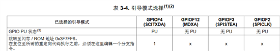
硬件上GPIOF4引脚是悬空的,
我在程序把GPIOF4设置为输入引脚
在线仿真在Expression看到输入值为1,如下图
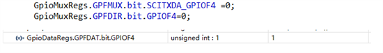
因此我猜引导模式设置为跳转到闪存
您看还有可能是什么别的原因么?


